
Automatic charging system of semiconductor packaging equipment

A technology for automatic feeding and packaging equipment, which is applied in semiconductor/solid-state device manufacturing, transportation and packaging, and conveyor objects. It can solve problems that affect the process and finished product quality, affect production efficiency, and occupy less space. Production efficiency and equipment utilization efficiency, no space occupation, stable operation effect

Active Publication Date: 2012-07-04
NANTONG FUJITSU MICROELECTRONICS
View PDF0 Cites 0 Cited by
  • Summary
  • Abstract
  • Description
  • Claims
  • Application Information

AI Technical Summary

Problems solved by technology

[0003] The current automatic feeding equipment is bulky, and it is difficult for packaging factories with high space utilization to achieve economical use of space; at the same time, the existing automatic feeding equipment has complex structures, high failure rates, manufacturing costs, and maintenance. The cost is high; in addition, due to the complex structural design, it often takes a lot of time to replace the feeding parts when producing products of different specifications, which has a certain impact on production efficiency
[0004] Although the traditional manual loading method occupies less space, it is inefficient, and it is easy to twist the frame or carrier board for semiconductor packaging during manual transfer, which will affect the subsequent process and the quality of the finished product

Method used


Image

  • Automatic charging system of semiconductor packaging equipment
  • Automatic charging system of semiconductor packaging equipment
  • Automatic charging system of semiconductor packaging equipment

Examples


Embodiment Construction

[0022] In the following description, numerous specific details are set forth in order to provide a thorough understanding of the present invention. However, the present invention can be implemented in many other ways different from those described here, and those skilled in the art can make similar extensions without violating the connotation of the present invention, so the present invention is not limited by the specific implementations disclosed below.

[0023] Secondly, the present invention is described in detail by means of schematic diagrams. When describing the embodiments of the present invention in detail, for convenience of explanation, the schematic diagrams are only examples, which should not limit the protection scope of the present invention.

[0024] The specific embodiments of the present invention will be described in detail below in conjunction with the accompanying drawings.

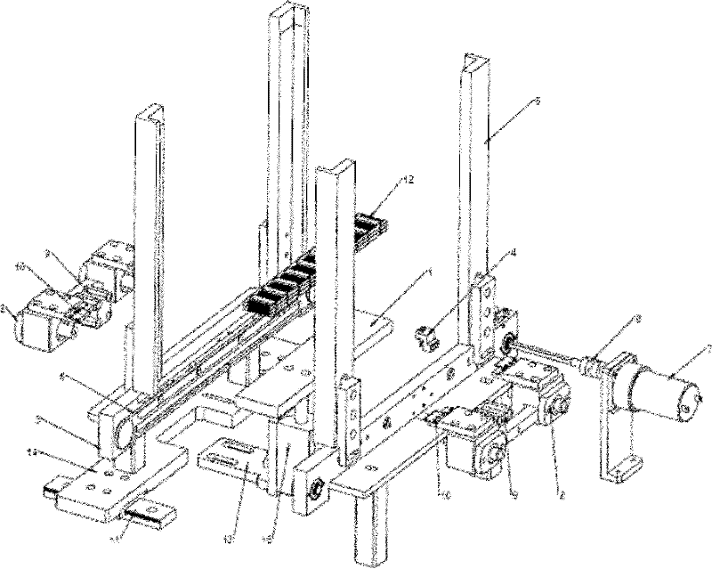
[0025] Such as figure 1 As shown, the automatic feeding system for semiconductor...


PUM


Abstract

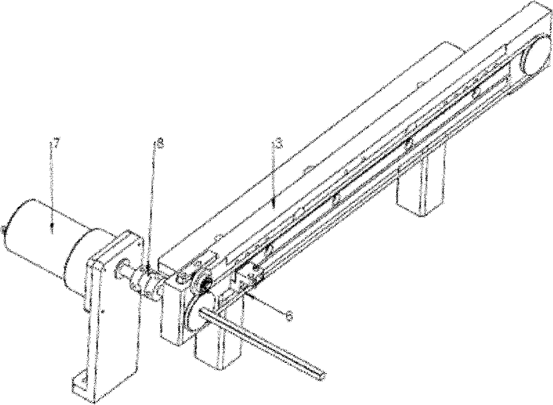
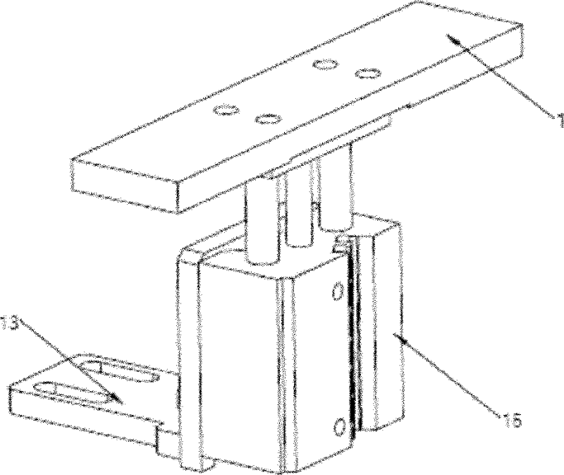
The invention relates to an automatic charging system of semiconductor packaging equipment. The system mainly comprises a conveying device, a track adjusting device, a basket, an ejection device, a distribution device, a power device and a track sensor. Compared with the prior art, the automatic charging system which the invention requests to protect has the following beneficial effects: the ejection device is used for conveying the whole group of frames or carrier plates to the assigned positions and then the distribution device is used for realizing single separation of the frames or the carrier plates to realize full automatic charging of the equipment; the system has a simple structure, does not occupy space, is stable to operate, has low cost and greatly improves the production efficiency and the equipment utilization efficiency; and the structure of the system is easy to adjust when different products are processed.

Description

technical field [0001] The invention relates to semiconductor technology, in particular to an automatic feeding system for semiconductor packaging equipment. Background technique [0002] In the semiconductor packaging process, the product has to go through the process of loading, operation and unloading in each process. [0003] The current automatic feeding equipment is bulky, and it is difficult for packaging factories with high space utilization to achieve economical use of space; at the same time, the existing automatic feeding equipment has a complex structure, high failure rate, manufacturing costs, and maintenance. The cost is very high; in addition, due to the complex structure design, it often takes a lot of time to replace the feeding parts when producing products of different specifications, which has a certain impact on production efficiency. [0004] Although the traditional manual loading method occupies less space, it is inefficient, and it is easy to twist ...

Claims


Application Information

Patent Timeline
Patent Type & Authority Patents(China)
IPC IPC(8): H01L21/56H01L21/677
Inventor 赵新民
Owner NANTONG FUJITSU MICROELECTRONICS
Features
  • Generate Ideas
  • Intellectual Property
  • Life Sciences
  • Materials
  • Tech Scout
  • Unparalleled Data Quality
  • Higher Quality Content
  • 60% Fewer Hallucinations
Learn More