Method for manufacturing circuit board with superouter fitting

A production method and circuit board technology, applied in the direction of printed circuit manufacturing, printed circuits, printed circuit components, etc., can solve the problems of slow lamination speed and low production efficiency of circuit boards, so as to improve production efficiency and speed up lamination speed. Effect

Inactive Publication Date: 2011-08-31
AVARY HLDG (SHENZHEN) CO LTD +1
View PDF3 Cites 4 Cited by
  • Summary
  • Abstract
  • Description
  • Claims
  • Application Information

AI Technical Summary

Problems solved by technology

This type of over-shaped accessories is usually bonded to a single circuit board unit one by one after cutting and forming, so that the fitting speed of the accessories is slow, and the production efficiency of the circuit board with over-shaped accessories is low.

Method used


Image

  • Method for manufacturing circuit board with superouter fitting
  • Method for manufacturing circuit board with superouter fitting
  • Method for manufacturing circuit board with superouter fitting

Examples


Embodiment Construction

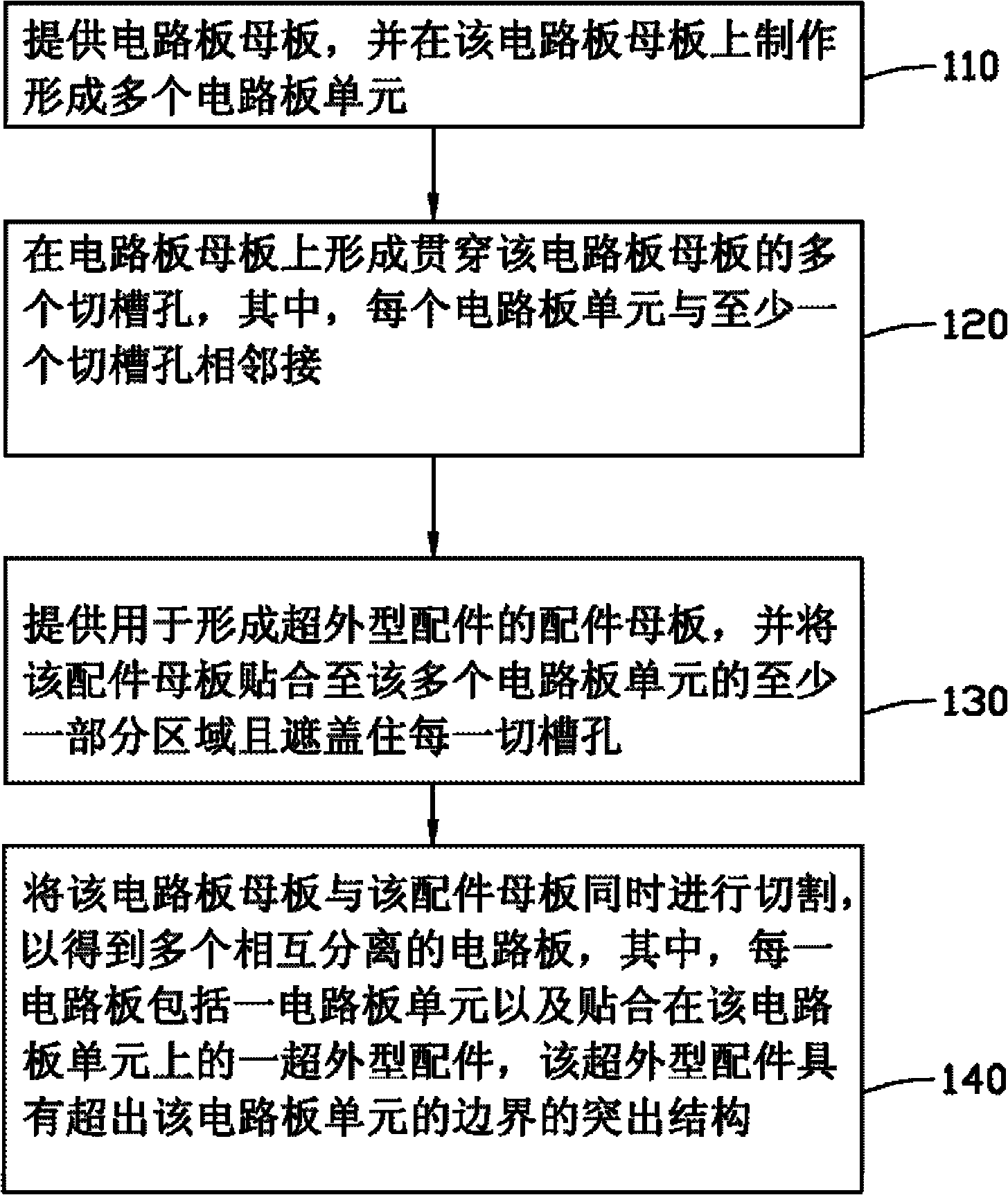
[0032] The manufacturing method of the circuit board with super-outside accessories of the technical solution will be further described in detail below in conjunction with the accompanying drawings and embodiments.

[0033] see figure 1 , the embodiment of the technical solution provides a method for manufacturing a circuit board with an oversized accessory, which includes the following steps:

[0034] In step 110, a circuit board motherboard is provided, and a plurality of circuit board units are formed on the circuit board motherboard.

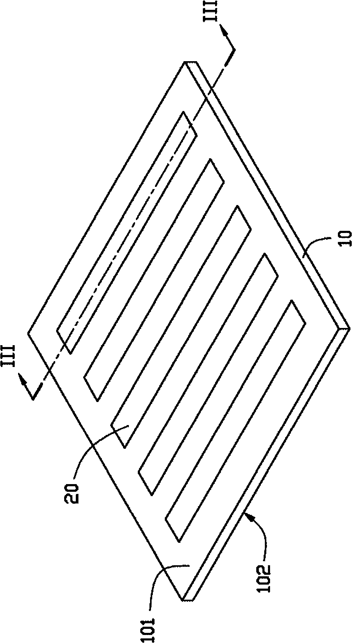
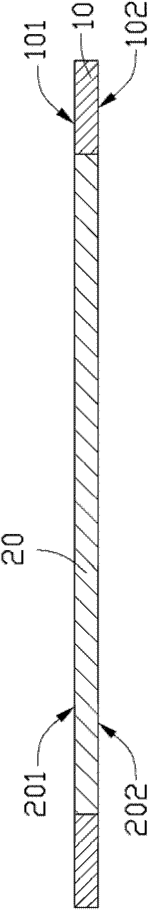
[0035] see Figure 2-3 , the circuit board motherboard 10 has a first surface 101 and a second surface 102 opposite to each other. Specifically, a plurality of circuit board units 20 can be formed on the circuit board motherboard 10 through a series of processes such as drilling, etching, exposure, development, pressing, and molding. Each circuit board unit 20 has a first surface 201 and a second surface 202 opposite to each other. In th...


PUM


Abstract

The invention provides a method for manufacturing a circuit board with a superouter fitting, which comprises the following steps of: providing a mother board of a circuit board and manufacturing and forming a plurality of circuit board units on the mother board of the circuit board; forming a plurality of slots penetrating through the mother board of the circuit board on the mother board of the circuit board, wherein each circuit board unit is adjacent to at least one slot; providing a fitting mother board for forming the superouter fitting and adhering the fitting mother board to at least one part of area of the circuit board units and covering each slot; and simultaneously cutting the mother board of the circuit board and the fitting mother board to obtain a plurality of mutually-separated circuit boards.

Description

technical field [0001] The invention relates to circuit board technology, in particular to a method for making a circuit board with super-outside fittings. Background technique [0002] With the rapid development of the electronic industry, the manufacturing technology of circuit boards, which are the basic components of electronic products, is becoming more and more important. The circuit board is generally made of a copper-clad substrate through a series of processes such as cutting, drilling, etching, exposure, development, pressing, and molding. For details, please refer to the article "Dielectric characterization of printed circuit board substrates" published by C.H.Steer et al. in Proceedings of the IEEE, Vol.39, No.2 (August 2002). [0003] At present, when making circuit boards, generally a plurality of circuit board units with the same structure and function are laid out on a larger circuit board motherboard. After the circuit board is manufactured, the plurality ...

Claims


Application Information

Patent Timeline
Patent Type & Authority Applications(China)
IPC IPC(8): H05K3/00H05K1/02
Inventor 邹立
Owner AVARY HLDG (SHENZHEN) CO LTD
Why Eureka
Try Eureka