Focusing ring and substrate carrying system

A focus ring and substrate technology, applied in the focus ring field, can solve the problems of low heat conduction efficiency between the focus ring and the base, low adhesion between the focus ring and the base, and difficulty in adjusting the temperature of the focus ring, so as to prevent changes in the heating mode Effect

Inactive Publication Date: 2011-09-21
TOKYO ELECTRON LTD
View PDF6 Cites 6 Cited by
  • Summary
  • Abstract
  • Description
  • Claims
  • Application Information

AI Technical Summary

Problems solved by technology

However, since the focus ring is placed only on the base, the closeness between the focus ring and the base is low, and the heat conduction efficiency between the focus ring and the base is low.
As a result, it is difficult to adjust the focus ring to the required temperature

Method used


Image

  • Focusing ring and substrate carrying system
  • Focusing ring and substrate carrying system
  • Focusing ring and substrate carrying system

Examples


Embodiment Construction

[0034] Hereinafter, embodiments of the present invention will be described in detail with reference to the drawings.

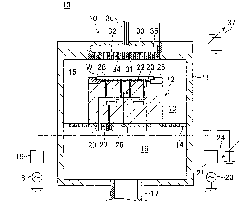
[0035] figure 1 It is a cross-sectional view schematically showing the structure of a plasma processing apparatus including a focus ring according to this embodiment. This plasma processing apparatus performs a plasma etching process on a wafer for a semiconductor device (hereinafter, simply referred to as a "wafer") as a substrate.

[0036] figure 1 Among them, the plasma processing apparatus 10 has, for example, a chamber 11 for accommodating a wafer W with a diameter of 300 mm, and a columnar susceptor 12 (mounting table) on which the wafer W for semiconductor devices is placed is disposed in the chamber 11 . In the plasma processing apparatus 10 , a side exhaust passage 13 is formed through the inner wall of the chamber 11 and the side surface of the susceptor 12 . An exhaust plate 14 is arranged in the middle of the side exhaust passage 13 .

[0037] ...


PUM

PropertyMeasurementUnit
thicknessaaaaaaaaaa
thicknessaaaaaaaaaa
thicknessaaaaaaaaaa

Abstract

The invention provides a focusing ring provided with a heat conduction plate with a film thickness suited for plasma treatment. In a plasma treatment device (10), the focusing ring (25) is enclosed on the periphery of the wafer W carried on a base (12) with a refrigerant chamber (26); a base contact surface (40) in contact with the base (12) and a heat conduction plate (38) formed on the base contact surface (40) are arranged in the plasma treatment device (10); the heat conductivity of the heat conduction plate (38) is in a range of from 0.5 to 5.0 W / m.K; the heat conduction plate (38) comprises silicon-containing heat-resistant adhesive and rubber; the adhesive and rubber contain a ceramic filler of oxide, nitride or carbide mixed therein in a content of 25-60% by volume; the film thickness of the heat conduction plate (38) is more than 40 mum and less than 400 mum.

Description

technical field [0001] The present invention relates to a focus ring and a substrate mounting system, and more particularly to a focus ring configured with the substrate mounting system to surround the periphery of a substrate. Background technique [0002] When performing plasma processing, such as etching, on a wafer as a substrate, since the etching rate of each part of the wafer is affected by the temperature of each part, it is required to maintain the temperature of the entire surface of the wafer uniformly during the etching process. . [0003] A substrate processing apparatus for performing an etching process on a wafer includes a decompressible chamber for accommodating a wafer, and a substrate mounting system for mounting the wafer disposed in the chamber. Plasma is generated in the depressurized chamber, and the plasma etches the wafer. The substrate mounting system has a cylindrical susceptor on which a wafer is placed on top, and a focus ring surrounding the p...

Claims


Application Information

Patent Timeline
Patent Type & Authority Applications(China)
IPC IPC(8): H01J37/21H01J37/02H01J37/32C23F4/00H01L21/00
CPCH01L21/67248H01L21/67103H01J37/32165H01J37/32091H01L21/68735H01J37/32642H01L21/3065H05H1/46
Inventor 北岛次雄小林义之渡边淳冈田拓也
Owner TOKYO ELECTRON LTD
Why Eureka
Try Eureka