Wafer-grade packaging method of ultraviolet LED packaging structure

A technology of LED packaging and manufacturing methods, applied in the direction of electrical components, circuits, semiconductor devices, etc., can solve the problems of device performance degradation, device reliability degradation, and easy intrusion into the chip surface, so as to avoid damage, realize airtight reliability, Effect of improving device production efficiency

Inactive Publication Date: 2014-04-30
SUN YAT SEN UNIV
View PDF5 Cites 0 Cited by
  • Summary
  • Abstract
  • Description
  • Claims
  • Application Information

AI Technical Summary

Problems solved by technology

The biggest problem caused by this is that the external water vapor easily invades the surface of the chip, which will directly reduce the performance of the device or seriously reduce the reliability of the device.

Method used


Image

  • Wafer-grade packaging method of ultraviolet LED packaging structure
  • Wafer-grade packaging method of ultraviolet LED packaging structure
  • Wafer-grade packaging method of ultraviolet LED packaging structure

Examples


Embodiment 1

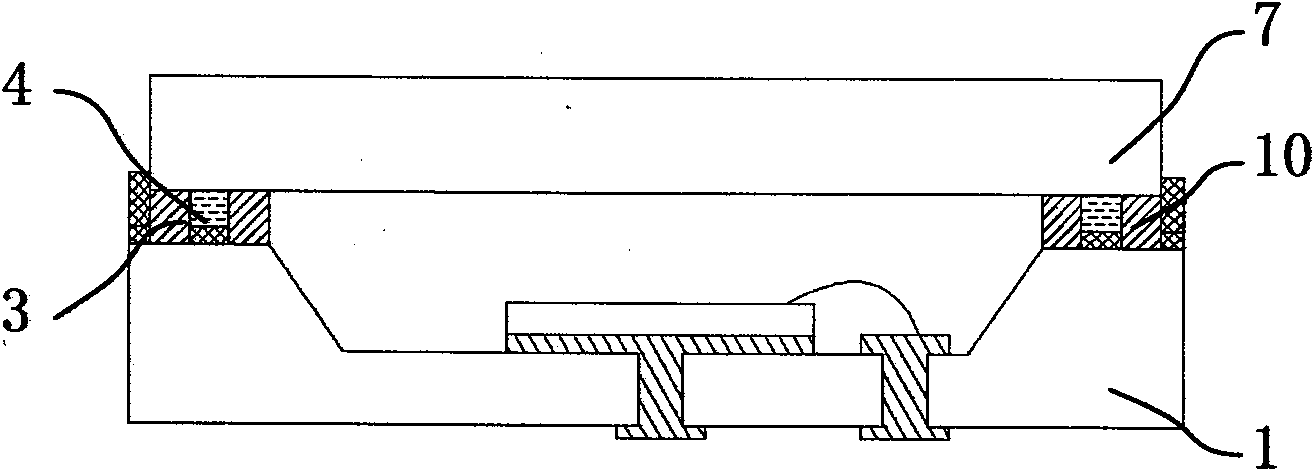
[0040] like figure 1As shown, it is a single-layer concave cup wafer-level ultraviolet LED packaging structure in this embodiment, including a packaging substrate 1, an LED chip 6 placed on the upper surface of the packaging substrate 1, and a packaging lens 7 packaged on the LED chip 6. The packaging The upper surface of the substrate 1 is provided with a concave cup 8 for accommodating the LED chip 6, and two conductive through-holes 9 are arranged at the bottom of the concave cup 8, and the conductive through-holes 9 are filled with two through holes connected to the electrodes of the LED chip 6. The hole electrode 5 is also provided with a bonding structure 10 for bonding the package lens on the wall of the concave cup 8. The bonding structure 10 includes a local heating circuit 4 and an airtight bonding substance 3 wrapped outside it. In addition, in The position corresponding to the local heating circuit 4 and the packaging substrate 1 is also provided with an insulating...

Embodiment 2

[0046] This embodiment is similar to Embodiment 1, the difference is that the LED chip 6 is a horizontal structure, which is fixed at the non-electrode position at the bottom of the concave cup 8, and the electrodes of the two chips 6 on the LED chip 6 are respectively connected by gold wires. on the two via electrodes 5 .

Embodiment 3

[0048] This embodiment is similar to Embodiment 2, except that the two chip electrodes of the LED chip are up and down, the LED chip is fixedly connected to one through-hole electrode, and the other chip electrode is connected to the other through-hole electrode through a gold wire.


PUM


Abstract

The invention discloses an ultraviolet LED packaging structure comprising a packaging substrate, an LED chip arranged on the upper surface of the packaging substrate and a packaging lens packaged on the LED chip, wherein the upper surface of the packaging substrate is provided with a concave cup for accommodating the LED chip, electric-conducting through holes are arranged at the bottom of the concave cup and are filled with through hole electrodes connected with the LED chip, the number of the through hole electrodes is same as that of the electric-conducting through holes, the wall of the concave cup is further provided with a bonding structure for bonding the packaging lens, and the bonding structure comprises a local heating loop and a hermetic bonding substance covering outside the local heating loop. The LED packaging structure disclosed by the invention realizes hermetic packaging by the bonding structure and is particularly suitable for working under severe environments with high humidity and the like, and the local heating loop is electrified for local heating to prevent damage to the chip due to heating, so that the hermetic reliability of a device is realized. The invention simultaneously provides a wafer-grade packaging method of the ultraviolet LED packaging structure, the wafer-grade manufacturing method has a simple technological process, can be used for effectively increasing the production efficiency of devices and is beneficial to complete cost reduction.

Description

technical field [0001] The invention relates to the field of LED packaging, in particular to an ultraviolet LED packaging structure and a wafer-level packaging manufacturing method thereof. Background technique [0002] The packaging process is the most important post-processing process in the semiconductor device manufacturing process. The quality of the packaging method has a direct and significant impact on the performance of the semiconductor device. Compared with common light sources, light-emitting diodes (LEDs) are currently the most promising solid-state light sources. However, regarding the performance of the LED device, the packaging structure of the LED chip and its process greatly restrict the luminous efficiency and lifespan of the LED device in use. [0003] In the traditional LED packaging process that uses silicon wafers as packaging substrates, the entire wafer is first cut into independent devices, and then each independent chip is packaged and tested, whi...

Claims


Application Information

Patent Timeline
Patent Type & Authority Patents(China)
IPC IPC(8): H01L33/48H01L33/62H01L33/52
Inventor 刘立林王钢钟健伟
Owner SUN YAT SEN UNIV
Why Eureka
Try Eureka