

Test probe
A test probe and probe insertion technology, applied in the field of test probes, can solve problems such as electrical contact damage
- Summary
- Abstract
- Description
- Claims
- Application Information
AI Technical Summary
Problems solved by technology
Method used
Image

Examples
Embodiment Construction
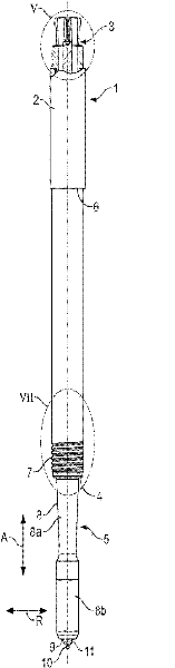
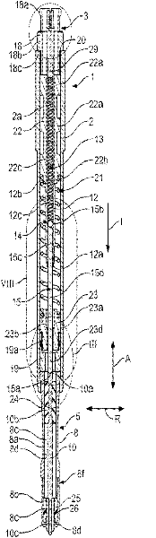
[0039] First, an embodiment of a test probe configured in accordance with the present invention will be referred to figure 1 A description is provided showing a schematic side view of an exemplary embodiment.
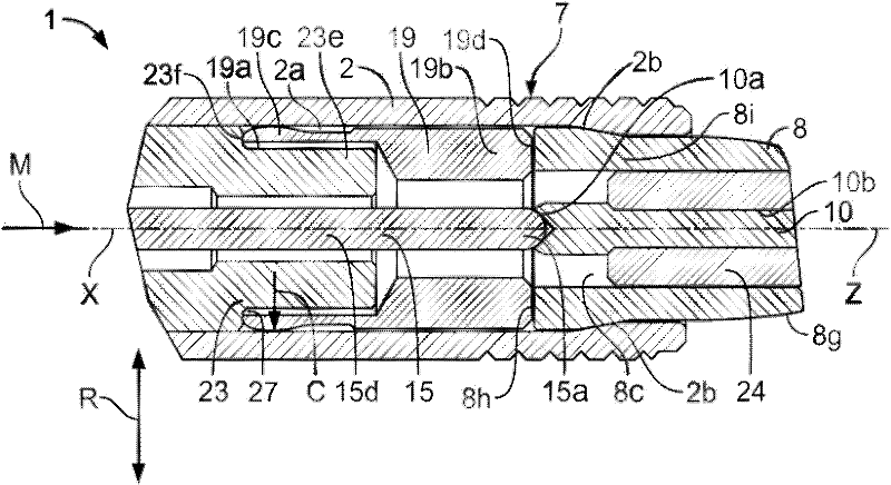
[0040] The test probe 1 comprises an elongated housing 2 . In order to connect the test probe 1 to a (not shown) test device, the test probe 1 is provided with a connector part 3 which is formed as a snap connection. The lower end of the housing 2 has an opening 4 in which the insertion part is seated.
[0041] The housing 2 has a shoulder 6 on its outer cylindrical surface which acts as a stop when the test probe is mounted on the adapter plate. For example, the smaller diameter lower part of the housing 2 can be inserted into the hole of the adapter plate until the shoulder 6 is in position on a corresponding shoulder of the adapter plate. At the lower end of the lower part of the housing 2, the housing 2 is provided with a helical thread for fixing the housing 2 t...
PUM
 Abstract
Description
Claims
Application Information