

Semiconductor luminescent device
A technology of light-emitting devices and semiconductors, applied in the direction of semiconductor devices, electrical solid devices, electrical components, etc., can solve problems affecting reliability, etc., and achieve the effect of preventing the deterioration of processability
- Summary
- Abstract
- Description
- Claims
- Application Information
AI Technical Summary
Problems solved by technology
Method used
Image

Examples
no. 1 example
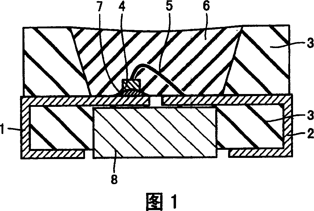
[0042] FIG. 1 is a cross-sectional view of a surface mount LED according to a first embodiment of the present invention.
[0043] The semiconductor light emitting device of the first embodiment includes: an LED chip 4; a first lead frame 1 on which the LED chip 4 is mounted; a second lead frame 2 electrically connected to the LED chip through a bonding wire 5 such as a gold wire 4; a resin portion 3 that surrounds the LED chip 4 and fixes the lead frame. The metal body 8 is located under the area where the LED chip 4 is mounted on the first lead frame 1 .
[0044] The first lead frame 1 and the second lead frame 2 are embedded in the resin portion 3 by insert molding. LED chips 4 are mounted on the first lead frame 1 with Ag paste 7 in between. Bonding wires 5 are connected to the second lead frame 2 . Therefore, the second lead frame 2 is mechanically and electrically connected to the LED chip 4 . The resin portion 3 is formed to surround the peripheries of the LED chip 4...
no. 2 example
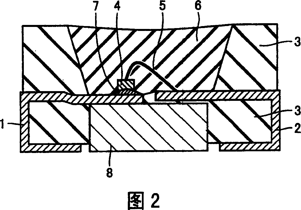
[0054] Fig. 2 is a cross-sectional view of a surface mount LED according to a second embodiment of the present invention.
[0055] The semiconductor light emitting device of the second embodiment is an improvement of the semiconductor light emitting device of the first embodiment. The metal body 8 is in contact with the first lead frame 1 .
[0056] For example, the first lead frame 1 on which the LED chip 4 is mounted is set lower than the second lead frame 2 so that contact with the metal body 8 is established. In the example shown in FIG. 2 , the first leadframe 1 is bent to make contact with the metal body 8 .
[0057] Therefore, the heat generated by the LED chip 4 is sequentially transferred through the first lead frame 1, the metal body 8 and the mounting board. There is no gap between the first lead frame 1 and the metal body 8 as in the first embodiment, so that the heat generated at the LED chip 4 is more effectively transferred to the mounting board. Although the...
no. 3 example
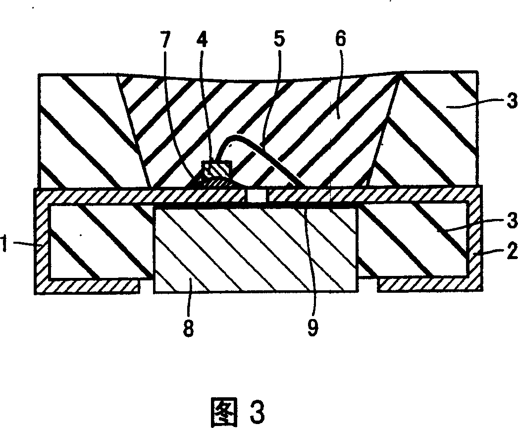
[0060] 3 is a cross-sectional view of a surface mount LED according to a third embodiment of the present invention.
[0061] The semiconductor light emitting device of the third embodiment is another improvement of the semiconductor light emitting device of the first embodiment. On the surface of the metal body 8 is provided an electrically insulating treated portion 9 formed, for example, by applying an insulating film, an insulating coating, or by anodizing. The surface of the metal body 8 subjected to the insulation treatment forms contact with the first lead frame 1 and the second lead frame 2 .
[0062] In the semiconductor light emitting device of the second embodiment, whether a single LED chip or a plurality of LED chips is used, as long as the LED chips are located on the same lead frame, the heat generated by the LED chip 4 can be transferred to the mounting board, and the first lead There is no portion corresponding to the gap in the first embodiment between the fr...
PUM
 Abstract
Description
Claims
Application Information