Band-gap reference source circuit with stable low-offset and low-noise noise chopped wave

A reference source circuit, low-noise technology, applied in the direction of adjusting electrical variables, control/regulating systems, instruments, etc., to achieve the effect of 1/f noise reduction, accurate output voltage, and small output ripple

Inactive Publication Date: 2011-09-28
SHANGHAI SANDHILL MICROELECTRONICS
View PDF5 Cites 21 Cited by
  • Summary
  • Abstract
  • Description
  • Claims
  • Application Information

AI Technical Summary

Problems solved by technology

[0007] The present invention solves its technical problems by adopting the following technical solutions: a low-offset low-noise chopper-stabilized bandgap reference source circuit, comprising an operational amplifier, two mirror-image-set transistors and voltage-dividing resistors, the first mirror-image set The base and collector of the first transistor and the second transistor are connected to the ground terminal of the signal, the emitter and collector of the first transistor are connected in series with the first resistor and the second resistor, and the other end of the second resistor is connected to the output of the operational amplifier terminal, the emitter and collector of the second transistor are connected in series with the third resistor, the other end of the third resistor is connected to the output terminal of the operational amplifier, the common terminal of the first resistor and the second resistor is connected to the inverting input terminal of the operational amplifier, and the second resistor is connected to the inverting input terminal of the operational amplifier. The emitter of the second transistor and the common end of the third resistor are connected to the non-inverting input end of the operational amplifier, which is characterized in that: the common end of the first and second resistors, and the common end of the emitter of the second transistor and the third resistor are respectively connected to the modulator The input terminal, the two output terminals of the modulator are respectively connected to the input terminals of the operational amplifier, and the two output terminals of the operational amplifier are respectively connected to the input terminals of the demodulator, and the output terminal of the demodulator is connected to the input terminal of an RC low-pass filter. The output terminal of the RC low-pass filter is connected to the input terminal of a buffer, and a transmission gate circuit is connected between the input terminal and the other input terminal of the buffer, and the other input terminal of the buffer is also connected to another RC low-pass filter The input of the RC low-pass filter is connected to the output of the buffer

Method used


Image

  • Band-gap reference source circuit with stable low-offset and low-noise noise chopped wave
  • Band-gap reference source circuit with stable low-offset and low-noise noise chopped wave
  • Band-gap reference source circuit with stable low-offset and low-noise noise chopped wave

Examples


Embodiment Construction

[0025] The present invention will be further described below in conjunction with the embodiments and the accompanying drawings.

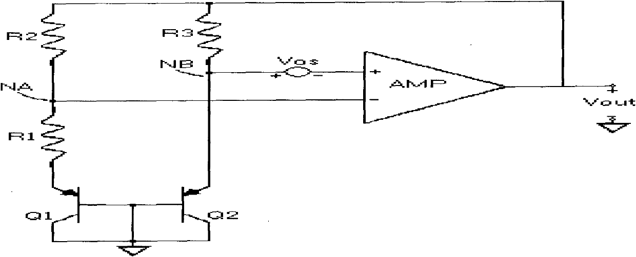
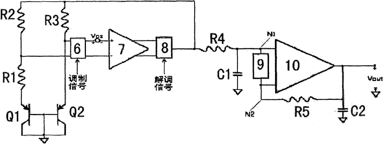
[0026] refer to figure 2 , the present invention includes an operational amplifier 7, two first transistor Q1 and second transistor Q2 set in mirror image, and voltage dividing resistors are R1, R2, R3, wherein the resistance values ​​of resistors R2 and R3 are the same.

[0027] The bases and collectors of the first and second transistors Q1 and Q2 are commonly connected to the signal ground, the emitter and collector of the first transistor Q1 are connected in series with the first resistor R1 and the second resistor R2, and the second resistor R2 The other end of the second transistor Q2 is connected to the output terminal of the operational amplifier 7, the emitter and the collector of the second transistor Q2 are connected in series with the third resistor R3, the other end of the third resistor R3 is connected to the output terminal of the op...


PUM


Abstract

The invention provides a band-gap reference source circuit with a stable low-offset and low-noise noise chopped wave, comprising an operational amplifier, a transistor arranged in the form of a mirror image and a divider resistor, wherein a modulator is connected in front of an input end of the operational amplifier while an output end of the operational amplifier is connected with a demodulator; an output end of the demodulator is connected with an input end of a RC low-pass filter; an output end of the RC low-pass filter is connected with an input end of a buffer; a transmission gate circuit is connected between two input ends of the buffer; another input end of the buffer is connected with an input end of another RC low-pass filter; and an output end of the RC low-pass filter is connected with an output end of the buffer. By using the invention, a signal is modulated at the input end of the operational amplifier and demodulated at the output end. The demodulated input signal is recovered while an equivalent offset voltage and 1 / F noise are modulated to a high frequency and then filtered by the low-pass filter, thereby reducing or even eliminating the influences of the offset voltage and the 1 / F noise on the precision and successfully solving the phenomenon of low output voltage precision caused by the offset voltage of the operational amplifier.

Description

【Technical field】 [0001] The invention relates to a bandgap reference source circuit in the field of large-scale analog integrated circuit design, in particular to a bandgap reference source circuit with low offset, low noise and chopper stability. 【Background technique】 [0002] figure 1 It is a typical bandgap reference functional structure diagram, which is composed of PNP transistors Q1, Q2, resistors R1, R2, R3, and operational amplifier AMP. The emitter area of ​​PNP transistor Q1 is n times that of transistor Q2, and Vos is the offset voltage. [0003] In the traditional bandgap reference circuit mentioned above, a feedback loop reference voltage is generated by the operational amplifier. The feedback loop keeps the voltages of the two input nodes of the operational amplifier equal, and the resistor R2=R3 makes the currents flowing through the PNP transistors Q1 and Q2 equal. Since the emitter area of ​​the transistor Q1 is n times that of Q2, a voltage of ΔVbe will...

Claims


Application Information

Patent Timeline
Patent Type & Authority Applications(China)
IPC IPC(8): G05F3/30
Inventor 肖国庆赵春和
Owner SHANGHAI SANDHILL MICROELECTRONICS
Why Eureka
Try Eureka