Error correction method, memory controller and memory storage system
A memory controller and error correction technology, applied in static memory, instruments, etc., can solve problems such as data loss and data cannot be corrected, and achieve the effect of improving the ability of error correction
- Summary
- Abstract
- Description
- Claims
- Application Information
AI Technical Summary
Problems solved by technology
Method used
Image
Examples
no. 1 example
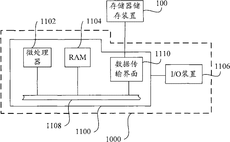
[0058] Figure 1A It is the host system using the memory storage device according to the first embodiment of the present invention.
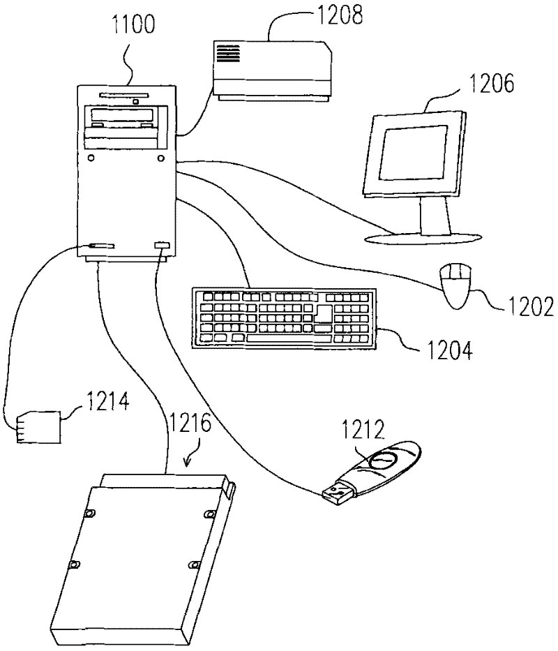
[0059] Please refer to Figure 1A , the host system 1000 generally includes a computer 1100 and an input / output (input / output, referred to as: I / O) device 1106 . The computer 1100 includes a microprocessor 1102 , a random access memory (random access memory, RAM for short) 1104 , a system bus 1108 and a data transmission interface 1110 . The input / output device 1106 includes such as Figure 1B mouse 1202, keyboard 1204, monitor 1206 and printer 1208. It is important to understand that Figure 1B The devices shown are not limited to the input / output device 1106, which may also include other devices.
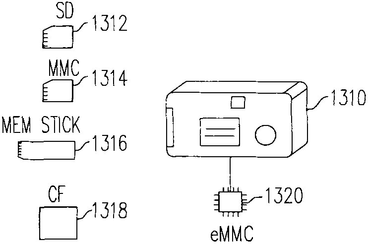
[0060] In the embodiment of the present invention, the memory storage device 100 is electrically connected with other components of the host system 1000 through the data transmission interface 1110 . Data can be written into or read from the mem...
no. 2 example
[0107] The memory storage device of the second embodiment is essentially the same as the memory storage device of the first embodiment, and only the differences are described here. The following will use the first embodiment figure 2 and image 3 The second embodiment will be described.
[0108] The memory management circuit 202 of the second embodiment will also Figure 4-11 The error correction mechanism, data access mechanism and memory management mechanism are shown to operate the memory die 106 . In this embodiment, in addition to performing the above-mentioned operation of opening the mother-child physical block and closing the operation of the mother-child physical block to write data, the memory management circuit 202 is also used to execute a random writing mode (Random Writing Mode) to write data .
[0109] Specifically, due to the programming specifications of the flash memory chip 106, it must be written from the first physical page of each physical block to t...
no. 3 example
[0128] The memory storage device of the third embodiment is essentially the same as the memory storage device of the first embodiment, and only the differences are described here. The following will use the first embodiment figure 2 and image 3 A third embodiment will be described.
[0129] The memory management circuit 202 of the third embodiment will also Figure 4-10 The data access mechanism and memory management mechanism are shown to operate the memory die 106 .
[0130] The memory chip 106 is an MLC NAND flash memory, so each memory cell can store multiple symbols. Specifically, when programming the memory cells of the SLC NAND flash memory, only a single-level program can be performed, so each memory cell can only store one symbol. The programming of the physical block of the MLC NAND flash memory can be divided into multiple stages. For example, taking a 2-layer storage unit as an example, the programming of the physical block can be divided into two stages. T...
PUM
 Abstract
Description
Claims
Application Information
 - R&D
- Intellectual Property
- Life Sciences
- Materials
- Tech Scout
- Unparalleled Data Quality
- Higher Quality Content
- 60% Fewer Hallucinations
Browse by: Latest US Patents, China's latest patents, Technical Efficacy Thesaurus, Application Domain, Technology Topic, Popular Technical Reports.
© 2025 PatSnap. All rights reserved.Legal|Privacy policy|Modern Slavery Act Transparency Statement|Sitemap|About US| Contact US: help@patsnap.com


