Integrated patch unit

A patch and luminous body technology, applied in the direction of electrical components, electric solid-state devices, semiconductor devices, etc., can solve the problems of complex circuit structure of full-color light-emitting units, light-emitting elements, driver chips and peripheral components that cannot be mounted as a whole, etc. Achieve the effect of mass production and easy mass production

Active Publication Date: 2011-10-05
GUANGZHOU CHAOWEI OPTOELECTRONICS TECH CO LTD
View PDF6 Cites 13 Cited by
  • Summary
  • Abstract
  • Description
  • Claims
  • Application Information

AI Technical Summary

Problems solved by technology

[0013] The purpose of the present invention is to overcome the problem that the circuit structure of the full-color light-emitting unit in the prior art is complicated, and its light-emitting element, driver chip and peripheral components cannot be mounted on the motherboard circuit as a whole

Method used


Image

  • Integrated patch unit
  • Integrated patch unit
  • Integrated patch unit

Examples


Embodiment 1

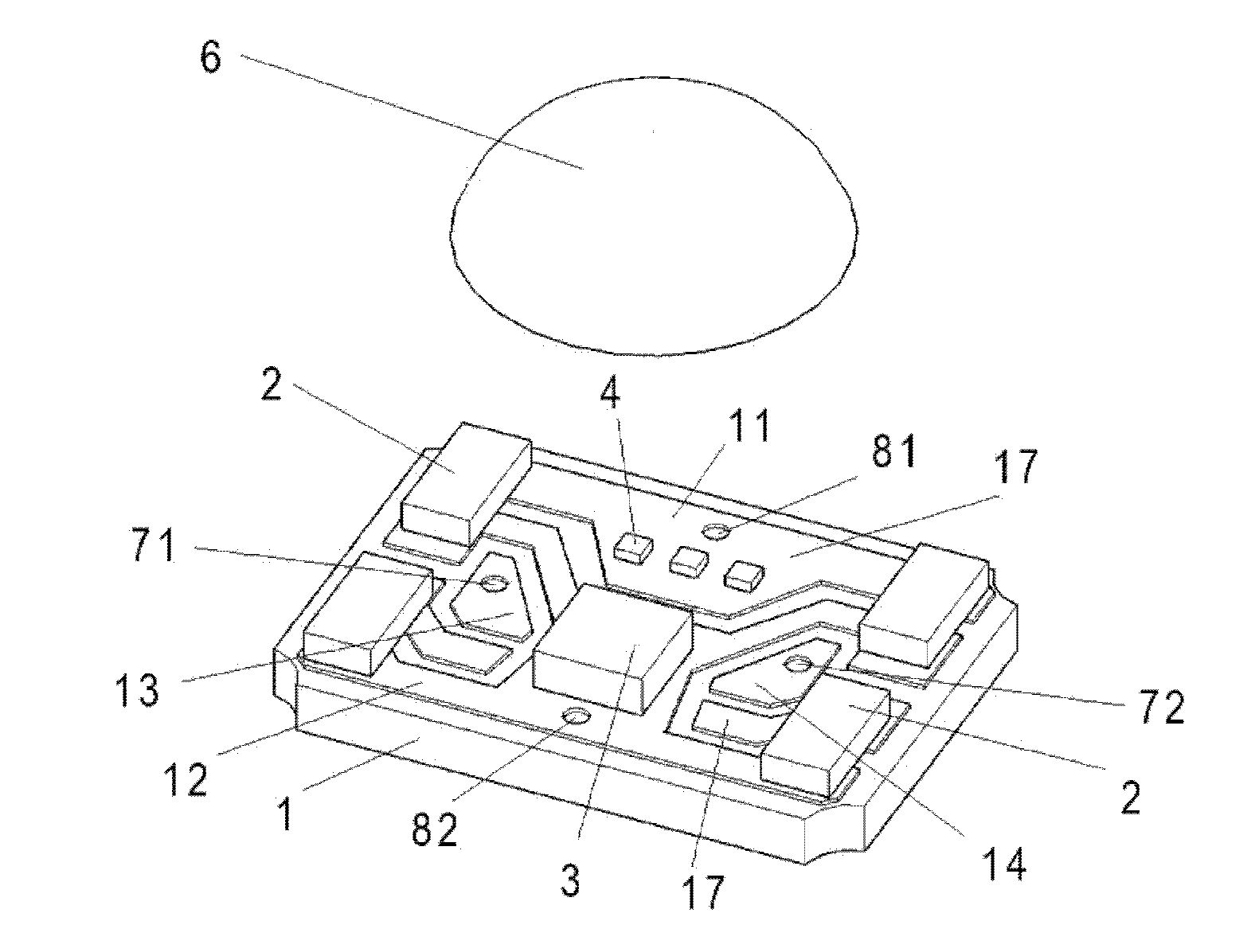
[0050] see figure 1 The integrated patch unit provided in this embodiment includes a circuit substrate 1, and the circuit substrate 1 at least includes a top circuit layer 17 and a bottom circuit layer (ie, Figure 13 The shown bottom circuit layer 18 is collectively referred to as "bottom circuit layer 18" hereinafter for convenience of description). The bottom circuit layer 18 functions as component patch leads, so it is also called a lead layer. The top circuit layer 17 is provided with peripheral components 2 , one power pole 11 , the other power pole 12 , signal input pole 13 , signal output pole 14 , luminous body 4 and driver chip 3 . details as follows:

[0051] One pole 11 of the power supply, the other pole 12 of the power supply, the signal input pole 13 and the signal output pole 14 are electrically connected to the bottom circuit layer 18 respectively; the luminous body 4 is electrically connected to the one pole 11 of the power supply; The signal output pole ...

Embodiment 2

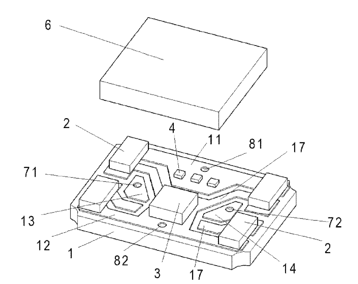
[0066] see image 3 , Figure 4 Compared with the above-mentioned first embodiment, the integrated patch unit provided in this embodiment differs in that: a dam 5 for potting and encapsulating the packaging material 6 is provided on the top circuit layer 17, and the dam 5 is used for The peripheral components 2 are isolated from the driving chip 3 and the luminous body 4 . An encapsulation groove 15 is formed in the dam 5 and on the top circuit layer 17 , and the encapsulation material 6 is poured into the encapsulation groove 15 .

[0067] Such as image 3 As shown, the dam 5 is a polygonal dam or an annular dam (for convenience of description, hereinafter, "polygonal dam or annular dam" is collectively referred to as a polygonal dam) by connecting several dams 51 end to end. Such as Figure 4 As shown, the polygonal dam is bonded on the circuit substrate 1 . The packaging groove 15 is formed on the circuit substrate 1 and is located in the dam 5; the driving chip 3 and ...

Embodiment 3

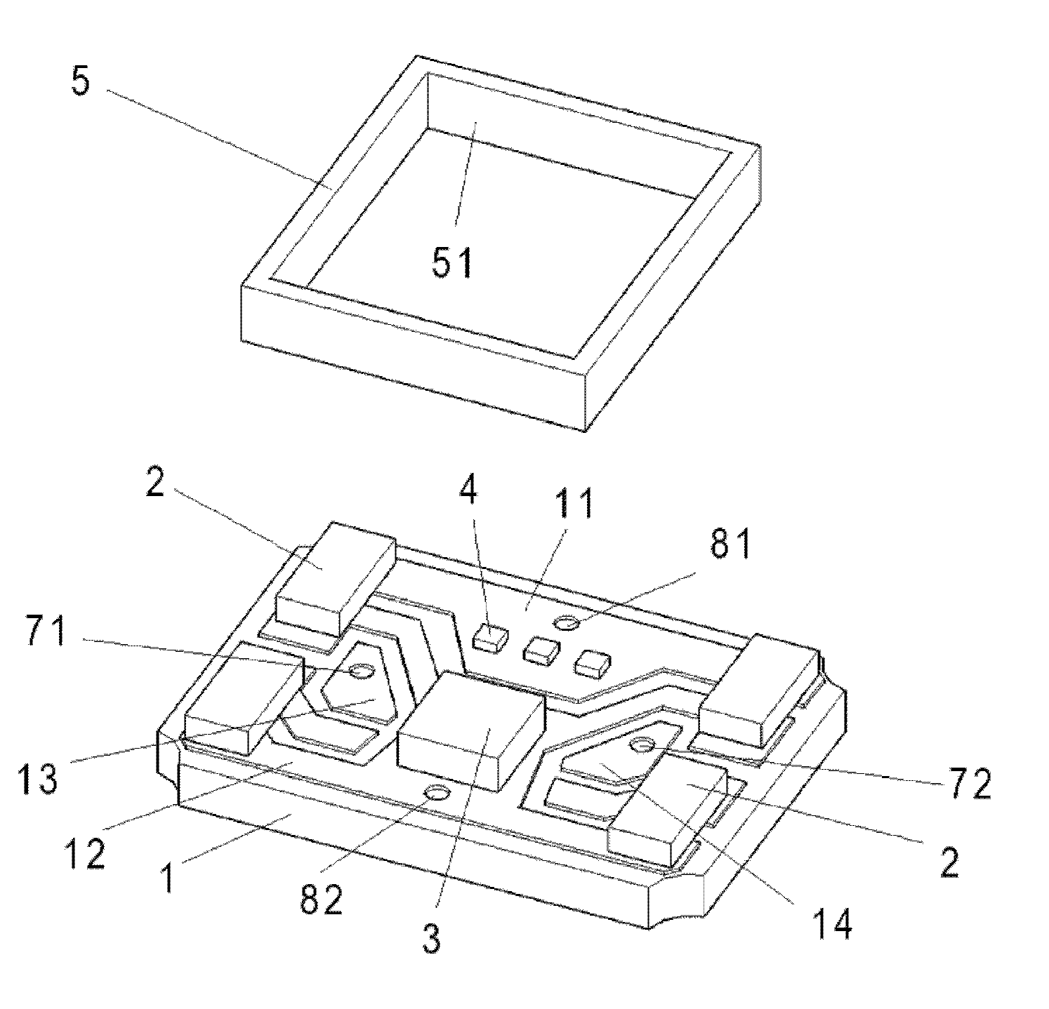
[0070] see Figure 5 , Figure 6 Compared with the above-mentioned second embodiment, the integrated patch unit provided by this embodiment is different in that: the dam 5 is provided with a positioning rod 55, and the conductive via hole 81 and the conductive via hole on the circuit board 1 are used to 82 as positioning holes.

[0071] Such as Figure 6 As shown, the locating rod 55 is connected with the dam 5 as a whole, and when the dam 5 and the circuit substrate 1 are mounted, the locating rod 55 is embedded on the circuit substrate 1; and the locating rod 55 is aligned with the positioning hole on the circuit substrate 1, so that The dam 5 is accurately attached to the circuit substrate 1 .

[0072] In this embodiment, the conductive vias 81 and 82 at the two poles of the power supply are used as positioning holes, and the positioning holes not only function as conductive vias, but also serve as positioning for the dam 5 . During specific implementation, the position...


PUM


Abstract

The invention discloses an integrated patch unit, comprising a circuit substrate and a light transmission packaging material, wherein the circuit substrate at least comprises a top circuit layer and a bottom circuit layer which are laminated with each other; a peripheral element as well as a power supply pole and the other power supply pole are arranged on the top circuit layer; the power supply pole and the other power supply pole are electrically connected with the bottom circuit layer; the top circuit layer is also provided with a luminous body electrically connected with the power supply pole and a driving chip which is electrically connected with the luminous body, the other power supply pole or the two power supply poles respectively; and the light transmission packaging material isarranged on the circuit substrate and covers the driving chip, the luminous body or the top layer of the whole circuit board. According to an embodiment of the invention, the driving chip, the luminous body and the peripheral element are integrated to form an integrated patch device so that the integrated patch unit provided by the invention has the characteristics of miniaturization, integrationand unitization and the mass production is much easier to realize.

Description

technical field [0001] The invention relates to the field of packaging technology, in particular to an integrated patch unit integrating a driving chip, a luminous body and peripheral components. Background technique [0002] The existing full-color light-emitting units (hereinafter referred to as light-emitting units, or units) generally use LED elements as light-emitting devices, and the full-color display is completed by LEDs of three primary colors. The unit includes driver integrated circuits (ICs) and peripheral components in addition to LED components. The existing light-emitting unit mainly adopts the circuit board manufacturing process, and the LED element, IC and peripheral components are welded on the circuit board to form an integrated structure. The IC and peripheral components are packaged in plug-in or patch type. However, no matter which packaging method is used, the volume of the light-emitting unit cannot be made small, for example, it is impossible to mak...

Claims


Application Information

Patent Timeline
Patent Type & Authority Applications(China)
IPC IPC(8): H01L33/48H01L33/62H01L25/16
CPCH01L2924/0002H01L23/3121H01L25/167
Inventor 蒋伟东
Owner GUANGZHOU CHAOWEI OPTOELECTRONICS TECH CO LTD
Why Eureka
Try Eureka