High-density flexible circuit board and manufacturing method thereof

A technology of flexible circuit boards and manufacturing methods, which is applied in the fields of printed circuit manufacturing, printed circuits, electrical components, etc., can solve the problems of low yield rate and achieve the effect of improving the yield rate

Active Publication Date: 2011-10-05
博罗县精汇电子科技有限公司
View PDF5 Cites 9 Cited by
  • Summary
  • Abstract
  • Description
  • Claims
  • Application Information

AI Technical Summary

Problems solved by technology

[0003] The invention provides a high-density flexible circuit board and a manufacturing method thereof. The circuit is prepared first, and then the drilling and copper plating processes are performed, so as to solve the technical problem of low yield rate caused by corrugated boards in the prior art.

Method used


Image

  • High-density flexible circuit board and manufacturing method thereof
  • High-density flexible circuit board and manufacturing method thereof
  • High-density flexible circuit board and manufacturing method thereof

Examples


Embodiment Construction

[0009] Specific embodiments of the present invention are described with reference to the above drawings.

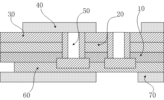
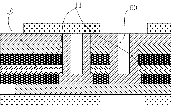
[0010] Depend on figure 1 with figure 2 It can be seen from the figure that this high-density flexible circuit board includes a polyimide base material 10, one side of the base material 10 is provided with a first conductive layer 20, and the first conductive layer 20 is provided with a deposited copper layer 30, The first covering layer 40 is provided on the said sinking copper layer 30, and a blind hole 50 is also drilled on the circuit board, and the said sinking copper layer 30 is along the inner wall of the blind hole 50, and the blind hole 50 The depth of the hole reaches the second conductive layer from the sinker and the copper plating layer 30 . The flexible substrate includes a flexible substrate and a conductive layer covering the flexible substrate, and the flexible substrate is polyimide. The manufacturing process of this high-density flexible circuit boa...


PUM


Abstract

The invention discloses a manufacturing method of a high-density flexible circuit board. The method comprises the following steps of: attaching a dry film to the surface of a conductive layer after a flexible substrate is cut; exposing and etching; pressing and laminating a covering film; and drilling a blind hole by using laser, depositing copper and plating copper. By using structural design and the manufacturing process, the problems of buckling of the high-density flexible circuit board, and wire break and short circuiting of the high-density flexible circuit board during circuit etching are effectively solved, and the yield of a product can be greatly increased.

Description

technical field [0001] The invention relates to a circuit board, in particular to the structural design and manufacturing process of a high-density flexible circuit board. Background technique [0002] At present, the process of producing high-density flexible circuit double-sided panels in the industry is: blanking→drilling→copper sinking→copper plating→filming, exposure→etching lines→covering film→lamination. Such a production process is used in the production of ordinary There is no problem with flexible circuit double-sided panels, but there are great difficulties in producing high-density flexible circuit double-sided panels: First, most high-density boards use very thin substrates, which are easy to wrinkle during operation; Second, due to the thickness of the board, the upper and lower boards or the mid-board are wrinkled during sinking and copper plating, so it is easy to make the dry film and the board surface not tightly bonded when the film is pasted, resulting in...

Claims


Application Information

Patent Timeline
Patent Type & Authority Applications(China)
IPC IPC(8): H05K3/00H05K1/00
Inventor 叶夕枫
Owner 博罗县精汇电子科技有限公司
Why Eureka
Try Eureka