Sine frequency modulation keying modulation communication method

A key modulation and sinusoidal technology, applied in the field of digital communication, can solve the problems of slow attenuation of carrier frequency points, unsuitable use, increase of system circuit complexity and resource occupation, etc.

Inactive Publication Date: 2011-10-19
HARBIN ENG UNIV
View PDF5 Cites 4 Cited by
  • Summary
  • Abstract
  • Description
  • Claims
  • Application Information

AI Technical Summary

Problems solved by technology

[0004] However, the amplitude of the very small LFM keying modulation waveform is not constant, so it is not suitable for use in some applications that require a constant amplitude modulation waveform
Analysis of the VMCK power spectrum shows that the attenuation from the carrier frequency point to both sides is relatively slow, and the sidelobe attenuation is not very large, so it is necessary to perform waveform shaping on the modulation waveform during modulation, and the transmitter includes an amplitude modulation part , which increases the complexity and resource occupation of the system circuit

Method used


Image

  • Sine frequency modulation keying modulation communication method
  • Sine frequency modulation keying modulation communication method
  • Sine frequency modulation keying modulation communication method

Examples


Embodiment Construction

[0041] The present invention is described in more detail below in conjunction with accompanying drawing example

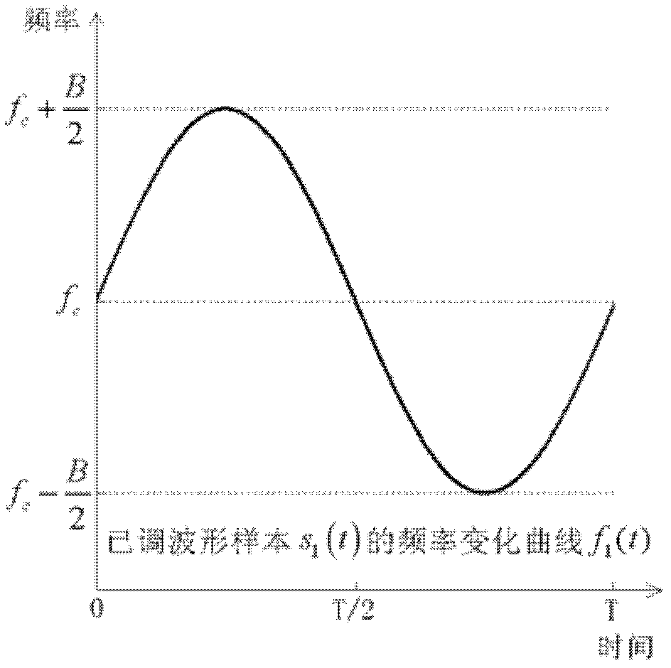
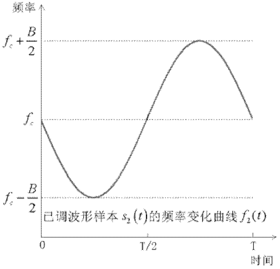
[0042] Fig. 1 is a schematic diagram of frequency variation of SNCK modulated signal waveform samples. It can be seen that the frequency change mode of the SNCK modulated signal is: when sending binary data "1", the frequency of the modulated signal waveform sample changes according to positive polarity sinusoidal; when sending data "0", the frequency of the modulated signal waveform sample changes according to Negative polarity sinusoidal change.

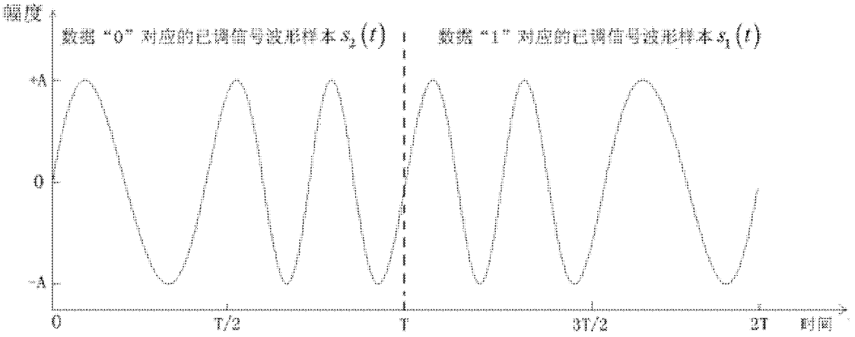
[0043] figure 2 It is a schematic diagram of the time-domain waveform of the SNCK modulated signal. It can be seen that the phase of the SNCK modulated signal is continuous and the frequency transition is smooth, which makes the smoothness of the modulated signal higher.

[0044] Fig. 3 is a graph of the power density spectrum of the SNCK modulated signal. Where Figure 3(a) is the bandwidth The power density spec...


PUM


Abstract

The invention provides a sine non-linear Chips keying modulation method. The method comprises the following steps: according to bandwidth B and data symbol cycle T of a modulated signal, calculating a modulation parameter D; according to center frequency fc, symbol cycle T and the modulation parameter D of the modulated signal, generating two frequency change function f1(t) and f2(t) corresponding to two waveform samples s1(t) and s2(t) of the modulated signal; according to the frequency change function f1(t) and f2(t), generating two waveform samples s1(t) and s2(t) of the modulated signal; according to mapping criterion between binary system digital modulated data and the modulated waveform samples, generating modulated signal siT(t) corresponding to ith information symbol; generating modulated signal s(t); and converting the modulated signal s(t) to simulation modulated signal through a digital-analog converter. According to the method, the two modulated waveform samples are non-linear Chips signals whose frequency change is sine type. Because of phase continuity of modulated signal and small difference between modulated signal waveform samples, the modulated signal generated through the sine non-linear Chips keying modulation method has extremely high energy concentration degree which facilitates realization of digital communication with high bandwidth efficiency.

Description

technical field [0001] The invention relates to a band-pass digital modulation method, which belongs to the field of digital communication. Background technique [0002] In digital communication, since the energy of the digital baseband signal is mainly concentrated in the low-frequency part, in order to realize long-distance wired or wireless transmission, it is necessary to use a high-frequency sine (cosine) wave as the carrier at the transmitter, and use the baseband signal to change a certain part of the carrier. These parameters make it change according to the change law of the baseband signal, realize the spectrum shift of the baseband signal, and make it suitable for information transmission. Recover the modulated signal with the corresponding circuit at the receiving end to realize demodulation. [0003] In 2007, Zheng Guoshen and others from Shanghai University applied for a patent for the ultra-narrowband communication method of very small chirp keying modulation,...

Claims


Application Information

Patent Timeline
Patent Type & Authority Applications(China)
IPC IPC(8): H04L27/12
Inventor 孙志国周彬曹雪郭黎利
Owner HARBIN ENG UNIV
Why Eureka
Try Eureka