Light-emitting element

A technology for light-emitting elements and light-emitting layers, applied in electrical components, semiconductor devices, circuits, etc., can solve the problems of difficulty and difficulty in improving the material constituting the transparent electrode, the conductivity of p-type GaN, and difficulty in luminous intensity, and achieve uniform luminous intensity. Effect

Inactive Publication Date: 2011-11-16
SANKEN ELECTRIC CO LTD
View PDF5 Cites 5 Cited by
  • Summary
  • Abstract
  • Description
  • Claims
  • Application Information

AI Technical Summary

Problems solved by technology

In the case where the resistance of the transparent electrode and the p-type GaN layer is negligible, such a problem does not occur, however it is practically difficult to increase the conductivity of the material constituting the transparent electrode and the p-type GaN, thereby reducing their resistance to negligible the degree is difficult
[0011] That is, in a light-emitting element having a structure in which two electrodes are formed on one surface of a semiconductor light-emitting functional layer, it is difficult to obtain uniform luminous intensity in the longitudinal direction.
Such a problem is particularly noticeable when the interval between two electrodes is wide.

Method used


Image

  • Light-emitting element
  • Light-emitting element
  • Light-emitting element

Examples


Embodiment Construction

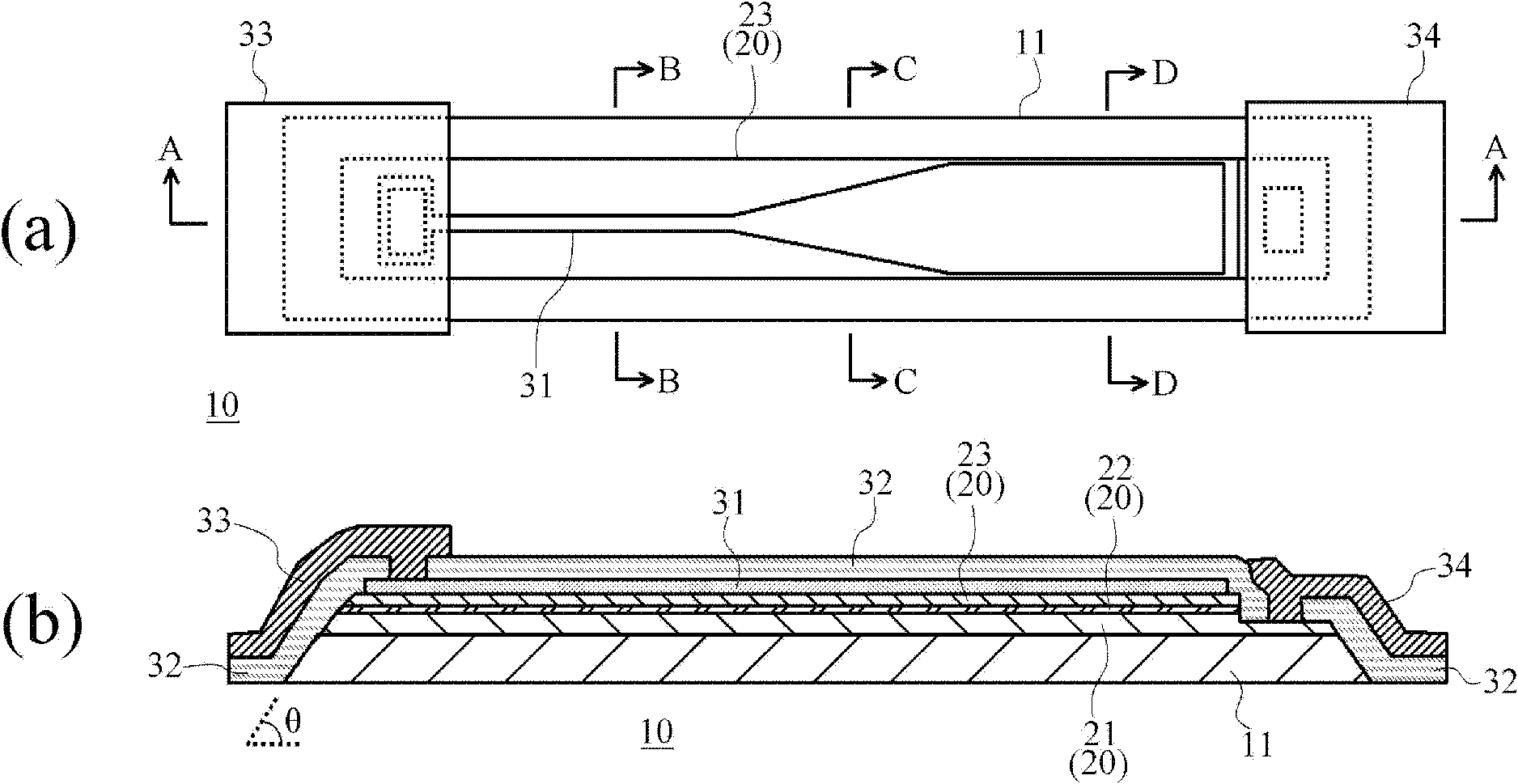
[0033] Hereinafter, a light emitting element according to an embodiment of the present invention will be described. In this light-emitting element, both the p-side electrode (anode) and the n-side electrode (cathode) are formed on one main surface side of the semiconductor light-emitting functional layer. In addition, the semiconductor light-emitting functional layer is formed in an elongated form in the direction from the p-side electrode toward the n-side electrode.

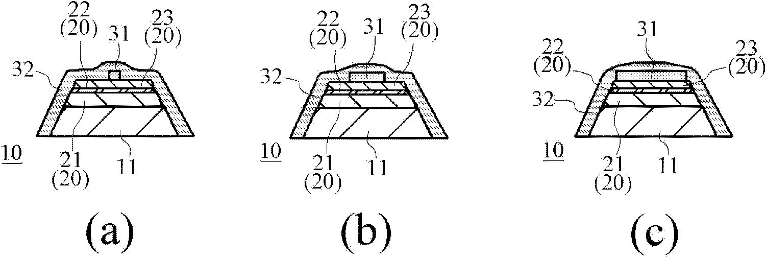
[0034] figure 1 It is a top view (a) of the light-emitting element 10 and a cross-sectional view (b) along the A-A direction thereof. and, figure 2 (a), (b), (c) are respectively figure 1 Cross-sectional views of B-B direction, C-C direction, and D-D direction in (a).

[0035] The semiconductor light-emitting functional layer 20 that emits light in the light-emitting element 10 is formed on the Si substrate 11, and has an n-type GaN layer (first semiconductor layer) 21, an MQW (Multi Quantum Well, multip...


PUM


Abstract

A light-emitting element forming a two-electrode structure on one face of a semiconductor light-emitting functional layer can obtain uniform luminous intensity along the length direction. The semiconductor light-emitting functional layer (20) which is formed on a Si substrate (11) has a laminating structure composed of a N type GaN layer (a first semiconductor layer) (21), a MQW layer (22), and a P type GaN layer (a second semiconductor layer) (23). A surface (a main face) of the P type GaN layer forms a transparent electrode (31) by extending from the other end part (the left end part) side towards the right end part side. An N-side electrode (34) is formed on the right end part side area. A P-side electrode (33) is formed on the left end part side area. The width of the transparent electrode (31) is gradually increasing from the left end part to the right end part. Therefore, the transparent electrode (31) limits the expansion of a current flowing vertically inside the MQW layer (22) on a side adjacent to the P-side electrode (33).

Description

technical field [0001] The present invention relates to the structure of a light-emitting element that emits light using a semiconductor as a structural material, and particularly relates to the structure of a linear light-emitting element. Background technique [0002] Semiconductor light emitting diodes (LEDs) are used for various purposes. For example, lighting equipment using light-emitting diodes has lower power consumption and lower heat generation than conventional incandescent bulbs and fluorescent lamps, and thus is expected to replace incandescent bulbs and fluorescent lamps in the future. Here, the p-type semiconductor layer and the n-type semiconductor layer in the LED are generally formed by epitaxial growth, ion implantation, and the like. Therefore, a pn junction surface is formed parallel to the surface of the semiconductor wafer, and electrodes connected to the p side and electrodes connected to the n side are assigned to the upper and lower surfaces of the...

Claims


Application Information

Patent Timeline
Patent Type & Authority Applications(China)
IPC IPC(8): H01L33/36H01L33/38
Inventor 杉森畅尚
Owner SANKEN ELECTRIC CO LTD
Why Eureka
Try Eureka