Welding pad structure for ball grid array packaging chip and multilayer printed circuit board for mobile phone

A ball grid array and multi-layer printing technology, which is applied to printed circuit components, electrical connection printed components, circuits, etc., to achieve the effect of reducing design difficulty, improving core competitiveness, and reducing the number of layers or series

Active Publication Date: 2011-11-23
HUIZHOU TCL MOBILE COMM CO LTD
View PDF3 Cites 9 Cited by
  • Summary
  • Abstract
  • Description
  • Claims
  • Application Information

AI Technical Summary

Problems solved by technology

[0007] Therefore, the existing technology still needs to be improved and developed

Method used


Image

  • Welding pad structure for ball grid array packaging chip and multilayer printed circuit board for mobile phone
  • Welding pad structure for ball grid array packaging chip and multilayer printed circuit board for mobile phone
  • Welding pad structure for ball grid array packaging chip and multilayer printed circuit board for mobile phone

Examples


Embodiment Construction

[0025] The specific implementations and examples of the present invention will be described in detail below in conjunction with the accompanying drawings. The described specific examples only use the specification parameters of 0.4mm pitch BGA packaging devices to explain the present invention, and are not intended to limit the specific implementation of the present invention. Way.

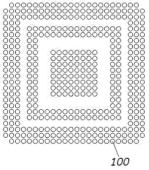
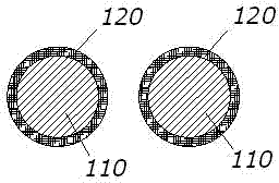
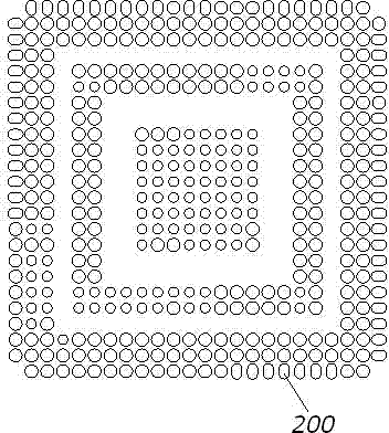
[0026] A pad structure of a ball grid array packaged chip of the present invention is arranged on the surface of a printed circuit board. One of its specific implementation methods is as follows: image 3 As shown, it includes a square ring grid array formed by a plurality of welding spots arranged at intervals; wherein, non-circular welding spots 200 are arranged in the outermost ring of welding spots of the grid array. At the same time, not all the solder joints 200 in the outermost circle of the grid array are set as non-circular solder joints 200 , and only need to be set in the solder joints ...


PUM


Abstract

The invention discloses a welding pad structure for a ball grid array packaging chip and a multilayer printed circuit board for a mobile phone. The welding pad structure for the ball grid array packaging chip comprises a plurality of welding spots which are mutually spaced and are used for forming a square circular grid array on the surface of the multilayer printed circuit board, wherein the square circular grid array is used for welding the ball grid array packaging chip; non-circular welding spots are arranged among the welding spots on an uttermost circle of the grid array; the length directions of the non-circular welding spots face to circular welding spots on an inner circle of the grid array; and a wire is arranged between two partially adjacent non-circular welding spots. The non-circular welding spots are arranged among the welding spots on the outer circle of a BGA (ball grid array) welding pad and a distance between adjacent welding spots on the outer circle is increased, thereby being capable of wiring from the middle part, connecting the circular welding spots on the inner circle of the grid array, reducing the design difficulty of the multilayer printed circuit board and particularly the design difficulty of a mobile phone main board, reducing the quantity of layer or level of the multilayer printed circuit board, virtually lowering the cost of mass production of the mobile phone main board and promoting the core competitiveness of a circuit board manufacturer.

Description

technical field [0001] The invention relates to the field of a ball grid array packaged chip and a mobile phone mainboard used therefor, and more specifically, relates to a pad structure of a ball grid array packaged chip and a multilayer printed circuit board of a mobile phone. Background technique [0002] In the 1990s, with the advancement of transistor technology and the continuous improvement of chip integration, the number of I / O pins increased sharply, power consumption also increased, and the requirements for integrated circuit packaging became more stringent. In order to meet the needs of the development of electronic products, BGA (Ball Grid Array Package, Ball Grid Array) packaging technology has begun to be applied to production. [0003] In recent years, global mobile communications have developed rapidly, and the penetration rate of mobile phones in developed countries has reached more than 70%, and in some areas it is even close to 100%. For the same type of ...

Claims


Application Information

Patent Timeline
Patent Type & Authority Applications(China)
IPC IPC(8): H05K1/11H01L23/498
Inventor 王佳
Owner HUIZHOU TCL MOBILE COMM CO LTD
Why Eureka
Try Eureka