Epitaxial substrate, preparation method of epitaxial substrate and application of epitaxial substrate as growing epitaxial layer

An epitaxial substrate and epitaxial growth technology, which is used in semiconductor/solid-state device manufacturing, thin material processing, electrical components, etc., can solve the problems of large size, high dislocation density, affecting the quality of epitaxial substrates, etc. The effect of reducing dislocation defects

Active Publication Date: 2011-11-30
TSINGHUA UNIV +1
View PDF8 Cites 31 Cited by
  • Summary
  • Abstract
  • Description
  • Claims
  • Application Information

AI Technical Summary

Problems solved by technology

However, in the prior art, grooves are usually formed on the surface of the sapphire substrate to form a non-flat epitaxial growth surface. However, due to the limitation of the process, the size of the grooves formed is relatively large, so the dislocation density in the obtained epitaxial substrate is still high. , thus affecting the quality of the epitaxial substrate

Method used


Image

  • Epitaxial substrate, preparation method of epitaxial substrate and application of epitaxial substrate as growing epitaxial layer
  • Epitaxial substrate, preparation method of epitaxial substrate and application of epitaxial substrate as growing epitaxial layer
  • Epitaxial substrate, preparation method of epitaxial substrate and application of epitaxial substrate as growing epitaxial layer

Examples


preparation example Construction

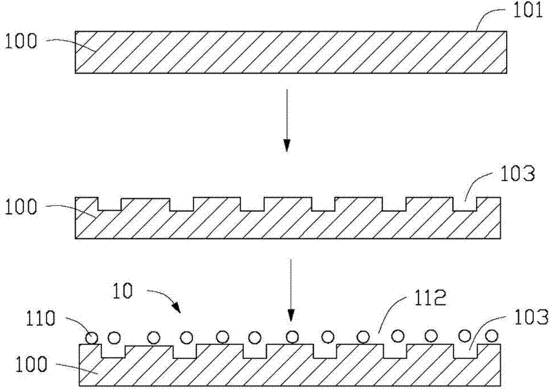
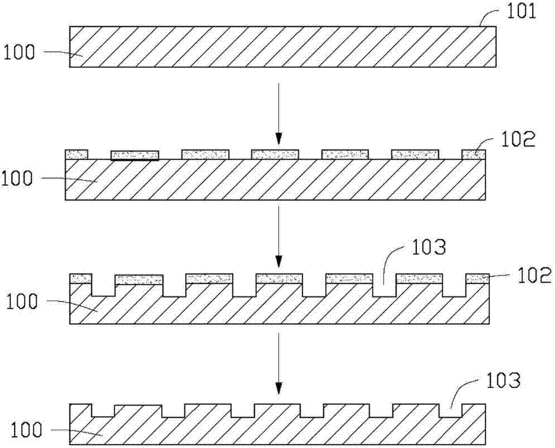
[0027] see figure 1 , an embodiment of the present invention provides a method for preparing an epitaxial substrate 10, which specifically includes the following steps:

[0028] Step S11, providing a substrate 100 having an epitaxial growth surface 101;

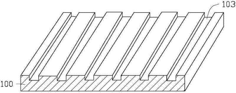
[0029] Step S12, etching the epitaxial growth surface 101 to form a patterned surface;

[0030] Step S13 , disposing a carbon nanotube layer 110 on the patterned epitaxial growth surface 101 .

[0031] In step S11 , the substrate 100 provides an epitaxial growth plane 101 for growing an epitaxial layer 120 . The epitaxial growth surface 101 of the substrate 100 is a molecularly smooth surface, and impurities such as oxygen or carbon are removed. The substrate 100 can be a single-layer or multi-layer structure. When the substrate 100 is a single-layer structure, the substrate 100 may be a single crystal structure, and has a crystal plane as the epitaxial growth plane 101 of the epitaxial layer 120 . The material of the su...


PUM

PropertyMeasurementUnit
widthaaaaaaaaaa
depthaaaaaaaaaa
widthaaaaaaaaaa

Abstract

The invention relates to an epitaxial substrate, which is used for growing an epitaxial layer. The epitaxial substrate comprises a substrate, wherein the substrate is provided with a patterned surface as an epitaxial growth surface. The epitaxial substrate further comprises a carbon nano tube layer covering the epitaxial growth surface of the substrate. The invention further provides a preparation method for the epitaxial substrate and the application of the epitaxial substrate as a grown epitaxial layer.

Description

technical field [0001] The invention relates to an epitaxial substrate for epitaxial growth, a preparation method of the epitaxial substrate and the application of the epitaxial substrate as a growing epitaxial layer. Background technique [0002] Epitaxial substrates, especially potassium nitride epitaxial substrates, are one of the main materials for making semiconductor devices. For example, in recent years, the preparation of GaN epitaxial wafers for light-emitting diodes (LEDs) has become a research hotspot. [0003] The gallium nitride epitaxial wafer means that under certain conditions, the gallium nitride material molecules are regularly arranged and oriented grown on an epitaxial substrate such as a sapphire substrate. However, the preparation of high-quality GaN epitaxial wafers has always been a difficult research point. Due to the difference in lattice constant and thermal expansion coefficient between gallium nitride and sapphire substrates, there are many dis...

Claims


Application Information

Patent Timeline
Patent Type & Authority Applications(China)
IPC IPC(8): H01L33/12H01L33/00
CPCH01L21/0237H01L21/0243H01L21/0265H01L21/02647H01L33/005H01L21/02639H01L21/02521H01L21/02444H01L33/20Y10T428/24562
Inventor 魏洋范守善
Owner TSINGHUA UNIV
Why Eureka
Try Eureka