Nitride semiconductor material and method of manufacturing nitride semiconductor crystal

A nitride semiconductor and manufacturing method technology, applied in semiconductor/solid-state device manufacturing, semiconductor devices, chemical instruments and methods, etc., can solve problems such as high price, GaN peeling, GaN cracks, etc., and achieve good surface flatness and crystal growth. High efficiency and the effect of omitting the grinding process

Inactive Publication Date: 2008-03-05
MITSUBISHI CHEM CORP
View PDF8 Cites 3 Cited by
  • Summary
  • Abstract
  • Description
  • Claims
  • Application Information

AI Technical Summary

Problems solved by technology

However, there is a problem that when a thick film of GaN is formed on a sapphire substrate or the like, cracks or cracks will occur on GaN, and GaN will peel off from the base substrate (see Non-Patent Document 1 and Non-Patent Document 2)
[0007] However, GaN substrates made by these methods cannot be said to have sufficient crystallization uniformity or stability, nor can they be said to be stable in quality, and are relatively expensive compared to sapphire substrates in the prior art

Method used


Image

  • Nitride semiconductor material and method of manufacturing nitride semiconductor crystal
  • Nitride semiconductor material and method of manufacturing nitride semiconductor crystal
  • Nitride semiconductor material and method of manufacturing nitride semiconductor crystal

Examples


Embodiment 1

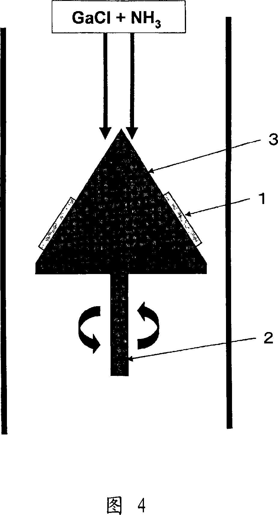
[0080] On a circular substrate with a thickness of 430 μm and a diameter of 5.08 cm (2 inches) with a slight inclination of 0.15° in the m-axis direction from the sapphire (0001) surface, 3 μm of undoped GaN was grown by MOVPE. Then, the substrate on which the GaN layer was grown was put into the HVPE apparatus, and the gas flow angle was set at 80° relative to the normal line of the substrate to grow the GaN layer. The growth conditions by the HVPE method were set as follows.

[0081] HCl partial pressure: 1.14kPa (1.13×10 -2 atm)

[0082] (Hereafter, HCl reacts with Ga metal to generate GaCl)

[0083] NH 3 Partial pressure: 4.58kPa (4.52×10 -2 atm)

[0084] Growth temperature: 1000°C (upstream side substrate end)

[0085] 970°C (downstream substrate end)

[0086] Carrier gas: H 2 (16(L))

[0087] Growth time: 5 hours

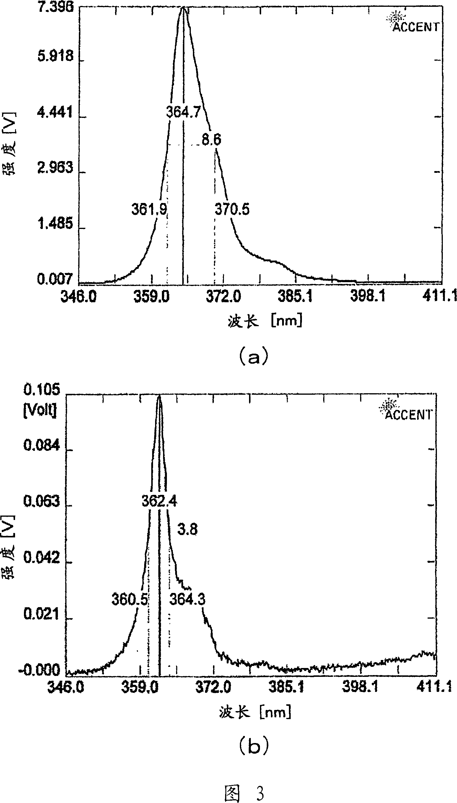
[0088] As shown in Figure 1, the crystalline thickness of the grown GaN layer was 170 μm, and no cracks, cracks, or spatially periodic defects were ...

Embodiment 2

[0090] On a circular sapphire (0001) substrate with a thickness of 430 μm and a diameter of 5.08 cm (2 inches), a 3 μm non-doped AlGaN layer was grown by the MOVPE method. The substrate for growing the AlGaN layer is set in the HVPE device, so that the surface of the substrate is parallel to the gas flow (with respect to the normal line of the substrate, the angle of the gas flow is 90°). The growth conditions of the HVPE method were set as follows.

[0091] HCl partial pressure: 1.14kPa (1.13×10 -2 atm)

[0092] (Below, HCl reacts with Ga metal to generate GaCl)

[0093] NH 3 Partial pressure: 4.58kPa (4.52×10 -2 atm)

[0094] Growth temperature: 1000°C (upstream side substrate end)

[0095] 970°C (downstream substrate end)

[0096] Carrier gas: H 2 (16(L))

[0097] Growth time: 5 hours

[0098] The crystal thickness of the grown GaN layer was 170 μm, and no cracks, cracks, or spatially periodic defects were concentrated on the surface. Usually, when only growing t...

Embodiment 3

[0100] On a circular sapphire (0001) substrate with a thickness of 430 μm and a diameter of 5.08 cm (2 inches), a non-doped GaN layer with a thickness of 1.5 μm was formed by the MOVPE method. A superlattice buffer layer in which five sets (each five layers) of InGaN layers and GaN layers each having a thickness of 10 nm were alternately inserted was formed thereon, and a non-doped buffer layer with a thickness of 1.5 μm was grown thereon. GaN layer. The substrate is set in the HVPE apparatus so that the substrate is parallel to the gas flow (with respect to the normal line of the substrate, the angle of the gas flow is 90°). The growth conditions of the HVPE method were set as follows.

[0101] HCl partial pressure: 1.14kPa (1.13×10 -2 atm)

[0102] (Below, HCl reacts with Ga metal to generate GaCl)

[0103] NH 3 Partial pressure: 4.58kPa (4.52×10 -2 atm)

[0104] Growth temperature: 1000°C (upstream side substrate end)

[0105] 970°C (downstream substrate end)

[01...


PUM

PropertyMeasurementUnit
thicknessaaaaaaaaaa
thicknessaaaaaaaaaa
thicknessaaaaaaaaaa

Abstract

A nitride semiconductor material wherein a first nitride semiconductor layer group is provided on a semiconductor substrate or a dielectric substrate is characterized in that a surface of the first nitride semiconductor group has an RMS of 5nm or less, an X-ray half width fluctuation within +-30%, a surface light reflectivity of 15% or more and its fluctuation at +-10% or less, and a thickness of the first nitride semiconductor group is 25[mu]m or more. The nitride semiconductor material has excellent uniformity and stability, is manufactured at a low manufacturing cost and is useful as a substrate for nitride semiconductor devices.

Description

technical field [0001] The present invention relates to nitride semiconductor materials suitable for use in semiconductor devices. In addition, the present invention also relates to a method for producing a nitride semiconductor crystal for producing the nitride semiconductor material. Background technique [0002] Conventionally, it is known that a compound semiconductor (hereinafter referred to as "nitride semiconductor") containing at least one element of Ga, Al, B, As, In, P, or Sb and N in its composition has a band gap of 1.9 to 6.2 eV. With such a wide range, it is expected to be used as a semiconductor material for light-emitting and photosensitive devices due to the wide range of band gap energy from ultraviolet light to visible light region. As a representative example of this nitride semiconductor, there is usually formula B x al y Ga z In 1-x-y-z A compound semiconductor represented by N (0≤x≤1, 0≤y≤1, 0<z<1, 0≤x+y+z≤1). Nitride semiconductor devices ...

Claims


Application Information

Patent Timeline
Patent Type & Authority Applications(China)
IPC IPC(8): H01L21/205C23C16/34H01L33/00
CPCH01L21/02581C23C16/34C30B25/18H01L21/02458H01L21/0262H01L21/02433C30B29/406H01L21/0242H01L21/02573H01L33/007H01L21/0237H01L21/0254C23C16/52
Inventor 清见和正堀江秀善石渡俊男藤村勇夫
Owner MITSUBISHI CHEM CORP
Why Eureka
Try Eureka