Optical substrate, substrate for semiconductor light emitting element, and semiconductor light emitting element

A technology for optical substrates and light-emitting components, which is applied in semiconductor devices, semiconductor/solid-state device manufacturing, electrical components, etc., and can solve problems such as reduced luminous efficiency, reduced external quantum efficiency, and reduced internal quantum efficiency

Inactive Publication Date: 2018-05-11
ASAHI KASEI KK
View PDF14 Cites 4 Cited by
  • Summary
  • Abstract
  • Description
  • Claims
  • Application Information

AI Technical Summary

Problems solved by technology

Due to this crystal dislocation defect, the internal quantum efficiency in the interior of the LED decreases, and as a result, the luminous efficiency of the LED decreases
[0004] In addition, since the refractive index of the GaN-based semiconductor layer is larger than that of the sapphire substrate, there is a problem that the light generated in the semiconductor light-emitting layer does not exit from the interface with the sapphire substrate at an angle greater than the critical angle, and becomes light-guided. mode and attenuation, resulting in a decrease in the external quantum efficiency

Method used


Image

  • Optical substrate, substrate for semiconductor light emitting element, and semiconductor light emitting element
  • Optical substrate, substrate for semiconductor light emitting element, and semiconductor light emitting element
  • Optical substrate, substrate for semiconductor light emitting element, and semiconductor light emitting element

Examples


Embodiment 1~ Embodiment 3

[0423] First, a substrate (optical base material) for LED is produced. The pattern of the LED substrate is made using nano-processed sheets. The nano-processed sheet will be described later. Prepare a 2-inch single-sided mirror c-plane sapphire and wash it. Next, the sapphire was placed on a hot plate at 120°C. Next, the nano-processed sheet was bonded to the sapphire using a lamination roll heated to 120°C. The bonding was performed at a line speed of 50 mm / sec under a pressure of 0.5 MPa. The sapphire to which the nano-processed sheet is laminated is irradiated with ultraviolet rays through the sapphire. Ultraviolet rays are irradiated by a UV-LED light source with a wavelength of 365nm, so the cumulative light quantity becomes 1500mJ / cm 2 Way to set. Next, the nano-processed sheet and sapphire were sandwiched by two parallel flat plates heated to 120°C. The clamping pressure is 0.3 MPa, and the time is 10 seconds. Then, it was cooled to room temperature by air cooling...

Embodiment 4

[0459] On the C-plane main surface of a 2-inch diameter sapphire single crystal substrate with a single-sided mirror-finished C-plane as the main surface, as in Example 1, the dry film resist using the nano-processed sheet was pressed In the plate printing method, a dry film resist layer formed with a convex mask pattern is formed.

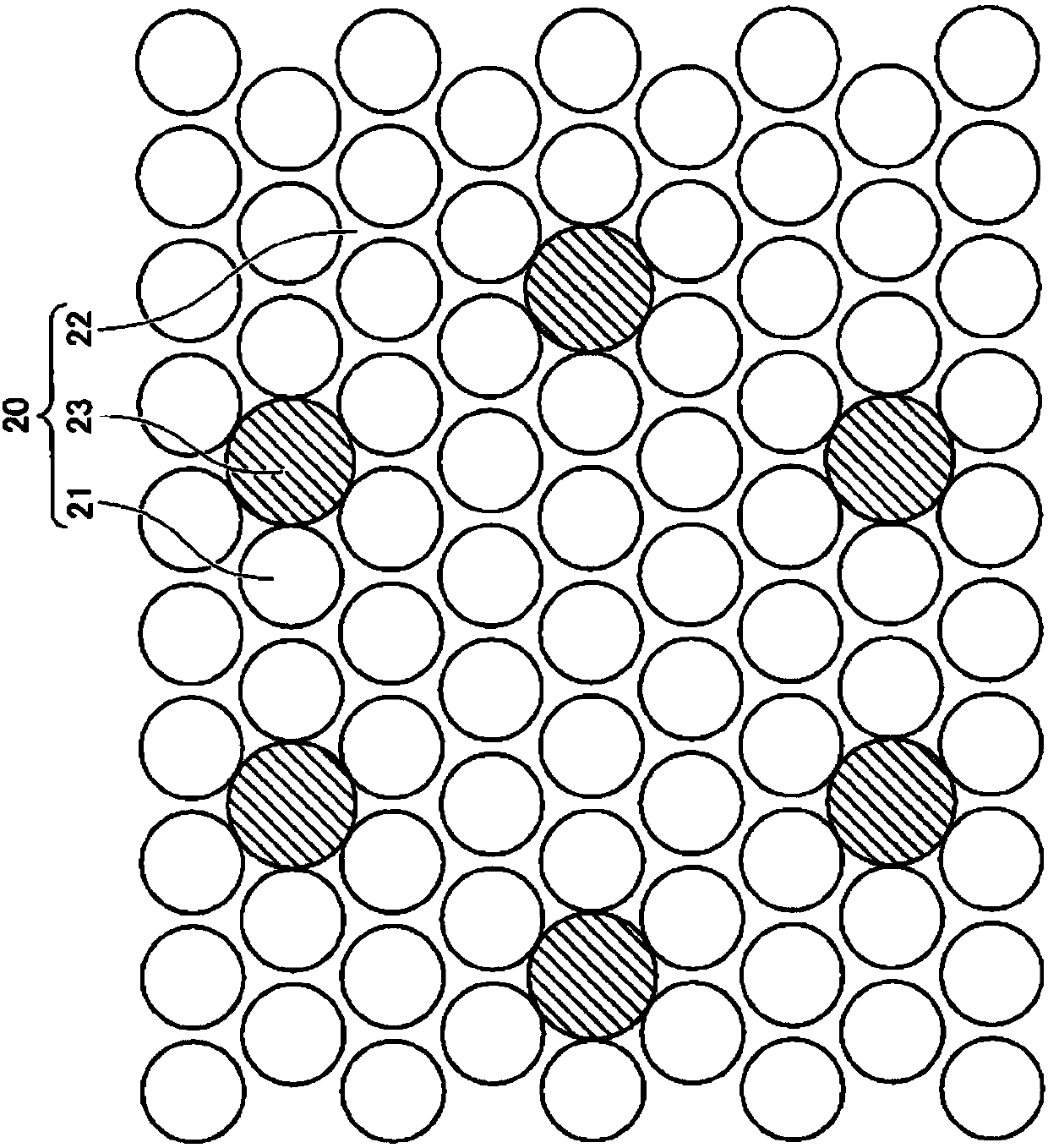
[0460] The mask pattern formed is and Figure 25 In the same convex pattern, the convex portions are arranged in a hexagonal grid with a lattice constant of 0.70 μm pitch, and the flat portions without the convex pattern are located at each vertex of a regular hexagon with one side of 1.40 μm and are repeatedly arranged.

[0461] Diameter of convex mask: 0.62μm

[0462] Height of convex mask: 1.47μm

[0463] Protruding mask pitch (Pn): 0.70μm

[0464] Plane pitch between convex masks (Pe): 1.40μm

[0465] Then, through the ICP dry etching device, using the mask pattern as a mask, through BCl 3 Gas and Cl 2 The gas mixture performs reactive ion etching to et...

Embodiment 5

[0477] The sapphire substrate produced in Example 4 was set in a MOCVD device to produce an LED. First, heat in a hydrogen atmosphere, after the surface is cleaned, and then form a film Al x Ga 1-x N(0≦x≦1) low temperature growth buffer layer. Next, a non-doped GaN layer is formed, and the composition ratio of the raw materials, the film formation temperature, and the film formation pressure are appropriately adjusted to fill the unevenness on the surface of the sapphire substrate with the GaN layer to obtain a flat undoped GaN layer.

[0478] The half-value width of the X-ray rocking curve (XRC-FWHM) of GaN (102) was measured, and the crystal quality of the undoped GaN layer was evaluated.

[0479] (XRC)

[0480] Device: X-Ray diffractometer (X-ray diffractometer)_SmartLab (manufactured by Rigaku)

[0481] Tube voltage: 45keV

[0482] Tube current: 200mA

[0483] Next, as the n-type GaN layer, Si-doped GaN is formed. Next, the strain absorbing layer is provided. Then, as a light-em...


PUM


Abstract

The purpose of the present invention is to provide a semiconductor film with which a semiconductor light emitting element having superior light emitting efficiency, especially compared to the prior art, can be manufactured with high yield, as well as a semiconductor light emitting element using the semiconductor film. The present invention is an optical substrate in which an uneven structure (20)is formed over part or an entirety of the principal surface, the uneven structure regularly including toothless sections. The uneven structure is constituted by projecting sections (21), inter-projecting sections bottom-sections (flat sections) (22), and recessed sections (23) (toothless sections) which have a flat surface positioned lower than the principal surface formed by the inter-projectingsections bottom-sections. The projecting sections are disposed at an average pitch P0, and the toothless sections are disposed at vertices of a regular polygon or on a side of the regular polygon thatconnects the vertices. The length of the side of the regular polygon is preferably longer than the average pitch P0.

Description

Technical field [0001] The present invention relates to an optical substrate having a concavo-convex structure, a semiconductor light-emitting element substrate for epitaxially growing semiconductor crystals on the surface thereof, and semiconductor light-emitting elements obtained from these substrates. Background technique [0002] Compared with conventional light-emitting devices such as fluorescent lamps or incandescent lamps, light-emitting diodes (LEDs), which are semiconductor light-emitting elements using a semiconductor layer, have characteristics such as miniaturization, improved power efficiency, and fast switching response, and because they are completely solid, Therefore, it has many advantages such as strong vibration resistance and long machine life. [0003] Among them, GaN-based semiconductor light-emitting elements represented by blue LEDs are manufactured by epitaxially growing an n-layer, a light-emitting layer, and a p-layer on a single crystal substrate. A sap...

Claims


Application Information

Patent Timeline
Patent Type & Authority Applications(China)
IPC IPC(8): H01L33/22
CPCH01L21/0243H01L21/0254H01L33/007H01L33/22H01L33/08H01L33/16H01L33/58
Inventor 室尾洋行山口布士人木山朋纪古池润前川知文
Owner ASAHI KASEI KK
Why Eureka
Try Eureka