Forming method of transistor

A transistor and gas technology, applied in the field of semiconductor manufacturing, can solve the problems such as the quality of embedded germanium and silicon needs to be improved, and achieve the effects of reducing the time for entering and exiting epitaxy equipment, reducing the generation cycle, and improving production efficiency

Active Publication Date: 2015-03-18
SEMICONDUCTOR MANUFACTURING INTERNATIONAL (BEIJING) CORP +1
View PDF3 Cites 4 Cited by
  • Summary
  • Abstract
  • Description
  • Claims
  • Application Information

AI Technical Summary

Problems solved by technology

[0005] The introduction of embedded silicon germanium technology can improve the carrier mobility of transistors to a certain extent, but in practical applications, it is found that in the process of forming transistors, the quality of embedded silicon germanium in transistors needs to be improved

Method used


Image

  • Forming method of transistor
  • Forming method of transistor
  • Forming method of transistor

Examples


Embodiment Construction

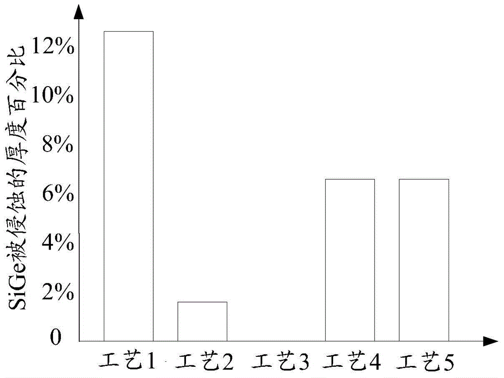
[0034] It can be seen from the background art that the quality of the germanium-silicon stress layer in the transistor formed in the prior art needs to be improved.

[0035] For this reason, the formation process of the transistor is studied, and the formation process of the transistor is used as an example. The formation process of the transistor includes the following steps, please refer to figure 1 :

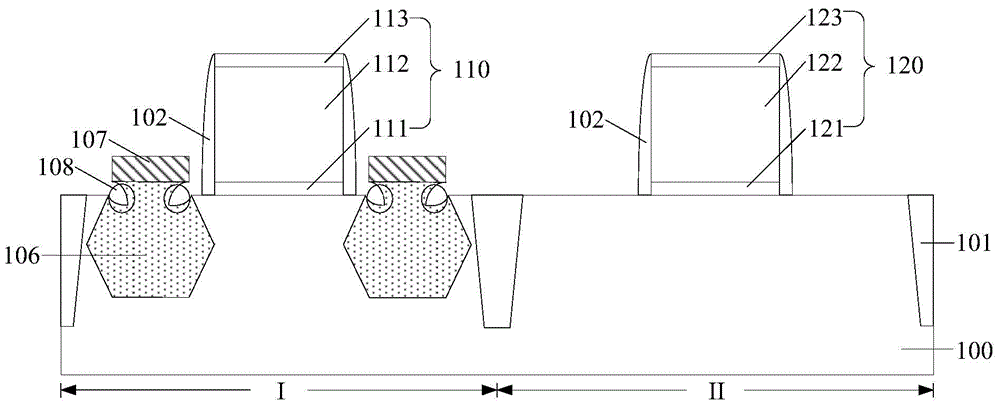
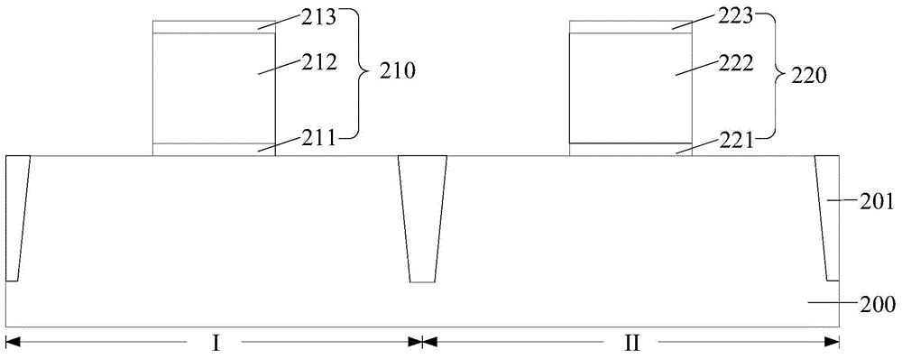
[0036] Provide a semiconductor substrate 100, an isolation structure 101 is formed in the semiconductor substrate 100, the semiconductor substrate 100 includes a PMOS region and an NMOS region, and a first gate structure 110 is formed on the surface of the semiconductor substrate 100 in the PMOS region , the second gate structure 120 is formed on the surface of the semiconductor substrate 100 in the NMOS region, and the first gate structure 110 includes a first gate oxide layer 111 located on the surface of the semiconductor substrate 100, a gate oxide layer located on the fi...


PUM


Abstract

A method is provided for fabricating a transistor. The method includes providing a semiconductor substrate having a first region; and forming a first gate structure on a surface of the semiconductor substrate in the first region. The method also includes forming trenches in the semiconductor substrate at both sides of the first gate structure; and forming a first stress layer with one surface lower than the surface of the semiconductor substrate in the trenches. Further, the method includes forming a second stress layer containing carbon atoms with a surface leveling with or higher than the surface of the semiconductor substrate on the first stress layer; and forming a source region and a drain region in the semiconductor substrate at both sides of the first gate structure.

Description

technical field [0001] The invention relates to the field of semiconductor manufacturing, in particular to a method for forming a transistor. Background technique [0002] With the continuous development of semiconductor technology, carrier mobility enhancement technology has been widely studied and applied. Improving the carrier mobility in the channel region can increase the driving current of MOS devices and improve the performance of the devices. [0003] In the existing manufacturing process of semiconductor devices, since stress can change the energy gap and carrier mobility of silicon materials, it has become an increasingly common means to improve the performance of MOS transistors through stress. Specifically, by properly controlling the stress, the mobility of carriers (electrons in NMOS transistors and holes in PMOS transistors) can be increased, thereby increasing the driving current, thereby greatly improving the performance of MOS transistors. [0004] At pres...

Claims


Application Information

Patent Timeline
Patent Type & Authority Applications(China)
IPC IPC(8): H01L21/336
CPCH01L21/823807H01L27/092H01L21/823814
Inventor 何永根
Owner SEMICONDUCTOR MANUFACTURING INTERNATIONAL (BEIJING) CORP
Why Eureka
Try Eureka