
Optical component and manufacturing method thereof

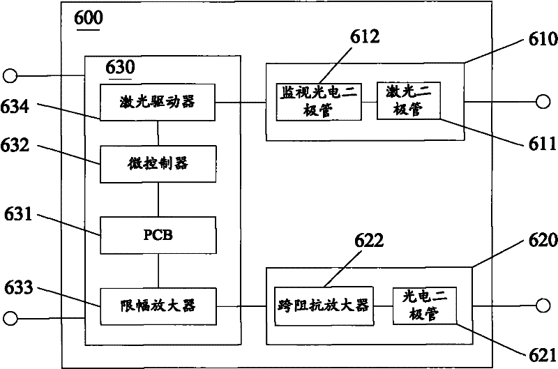
A manufacturing method and technology for optical components, applied in the field of optical communication, can solve problems such as affecting transmission signals, and achieve the effects of high-speed transmission with large bandwidth, simplified wiring design, and reduced manufacturing costs

Inactive Publication Date: 2011-12-07
SAE MAGNETICS (HK) LTD
View PDF6 Cites 3 Cited by
  • Summary
  • Abstract
  • Description
  • Claims
  • Application Information

AI Technical Summary

Problems solved by technology

For example, since the limiting amplifier is installed on the PCB, and the transimpedance amplifier is formed in the ROSA, when the transimpedance amplifier of the ROSA communicates with the limiting amplifier, a large amount of distributed capacitance will seriously affect the transmission signal
Moreover, serious transmission loss will also occur

Method used


Image

  • Optical component and manufacturing method thereof
  • Optical component and manufacturing method thereof
  • Optical component and manufacturing method thereof

Examples


Embodiment Construction

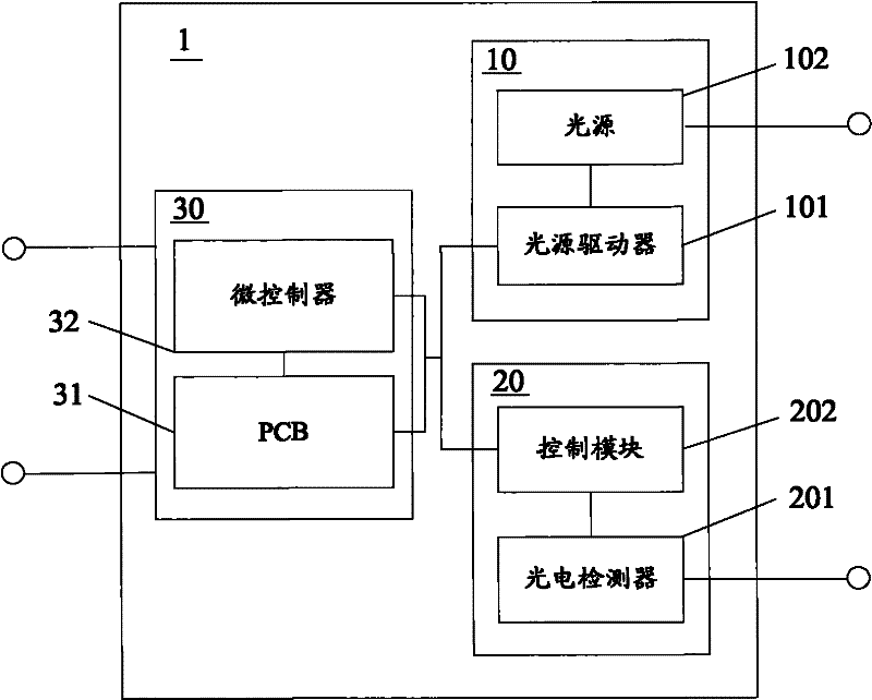
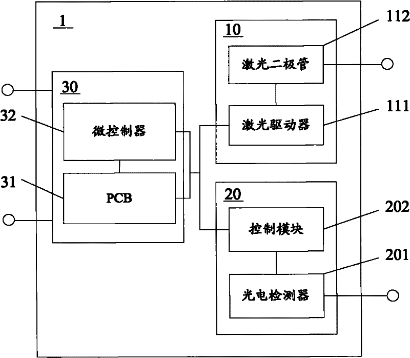
[0042] Several different preferred embodiments of the present invention will now be described with reference to the accompanying drawings, wherein like reference numerals in different drawings represent like parts. As mentioned above, the essence of the present invention is to integrate the transimpedance amplifier and the limiting amplifier into a control module, and embed it into the ROSA, and integrate the laser driver into the TOSA. This design makes optical components highly integrated to meet the requirements of high-speed transmission and large bandwidth in optical-electrical and electrical-optical conversion. On the other hand, since only the microcontroller IC is mounted on the PCB, the wiring design of the PCB is simplified, for example, the number of wiring layers can be reduced to four layers, while the prior art requires at least six layers. In addition, since the number of ICs is reduced, manufacturing costs are reduced accordingly. In addition, the present inve...


PUM


Abstract

The invention discloses an optical component, which includes a light transmitter component, a light receiver component and an electronic component respectively connected to the light transmitter component and the light receiver component. The light transmitter assembly includes a light source and a light source driver for driving the light source; the light receiver assembly includes a photodetector and a control module connected to the photodetector, the control module is at least composed of a transimpedance The amplifier and a limiting amplifier are integrated; the electronic component includes a printed circuit board and a microcontroller formed on the printed circuit board, and the microcontroller is connected to the light source driver and the control module respectively. The optical component of the present invention has a high degree of integration, thereby meeting the requirements for high-speed transmission and large bandwidth in optical-electrical and electric-optical conversion, simplifying the design of PCB and reducing manufacturing costs.

Description

technical field [0001] The invention relates to the field of optical communication, in particular to a highly integrated optical component and a manufacturing method thereof. Background technique [0002] In optical communication networks, optical components are often used to reduce manufacturing costs. For example, optical components are often used to transmit and receive optical signals in optical fibers. A common type of optical assembly includes multiple die elements incorporated in a packaged assembly. For example, if figure 1 As shown, a conventional optical assembly 600 includes an optical transmitter assembly (transmitter optical subassembly, TOSA) 610, an optical receiver assembly (receiver optical subassembly, ROSA), and an electronic assembly 630 connected to the TOSA 610 and the ROSA 620, respectively. [0003] The electronic assembly 630 includes a printed circuit board (PCB) 631 and a microcontroller 632 , a limiting amplifier 633 and a laser driver 634 resp...

Claims


Application Information

Patent Timeline
Patent Type & Authority Applications(China)
IPC IPC(8): G01D5/26
CPCH04B10/40Y10T29/49002
Inventor 黄永亮
Owner SAE MAGNETICS (HK) LTD
Learn More