Chemical vapor deposition with elevated temperature gas injection

A chemical vapor deposition, gas technology, used in gaseous chemical plating, electrical components, semiconductor/solid-state device manufacturing, etc., can solve problems such as limited operating conditions

Inactive Publication Date: 2011-12-07
VEECO INSTR
View PDF7 Cites 4 Cited by
  • Summary
  • Abstract
  • Description
  • Claims
  • Application Information

AI Technical Summary

Problems solved by technology

[0011] Prior to the present invention, however, the operating conditions that could be used were very limited

Method used


Image

  • Chemical vapor deposition with elevated temperature gas injection
  • Chemical vapor deposition with elevated temperature gas injection
  • Chemical vapor deposition with elevated temperature gas injection

Examples


Embodiment Construction

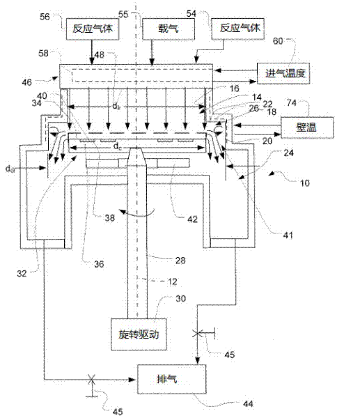
[0022] A device according to one embodiment of the present invention ( figure 1 ) includes a reaction chamber 10 with a central axis 12 . In this embodiment, axis 12 is generally vertical, as seen in a normal gravitational frame of reference. The inner walls of the reaction chamber 10 are generally in the form of surfaces that rotate about an axis 12 . In the flow region 14 at the top of the reaction chamber, an inner wall 16 exists approximately in the form of a cylinder with a diameter d concentric to the axis FR . The region 18, referred to herein as the "carrier region", has a cylindrical inner wall 20, which likewise generally has the form of a cylinder coaxial to the axis 12, with a diameter d CR greater than d FR , the reaction chamber has a downwardly facing transition surface 22 at the junction of the flow region and the carrier region. The reaction chamber likewise has an outlet region 24 located below the carrier region. The walls of the reaction chamber have...


PUM

PropertyMeasurementUnit
thicknessaaaaaaaaaa

Abstract

A chemical vapor deposition reactor and method. Reactive gases, such as gases including a Group III metal source and a Group V metal source, are introduced into a rotating-disc reactor and directed downwardly onto a wafer carrier and substrates which are maintained at an elevated substrate temperature, typically above about 400° C. and normally about 700-1100° C. to deposit a compound such as a III-V semiconductor. The gases are introduced into the reactor at an inlet temperature desirably above about 75° C. and most preferably about 100°-250° C. The walls of the reactor may be at a temperature close to the inlet temperature. Use of an elevated inlet temperature allows the use of a lower rate of rotation of the wafer carrier, a higher operating pressure, lower flow rate, or some combination of these.

Description

[0001] Cross References to Related Applications [0002] This application is a continuation-in-part of US Patent Application No. 12 / 291,350, filed November 6, 2008, the disclosure of which is incorporated herein by reference. technical field [0003] The invention relates to a chemical vapor deposition method and equipment. Background technique [0004] Chemical vapor deposition involves directing one or more gases containing chemical species onto the surface of a substrate so that the reacting species react and form a deposit on the surface. For example, compound semiconductors can be formed by epitaxial growth of semiconductor material on a substrate. The substrate is usually a disk of crystalline material, commonly referred to as a "wafer". Compound semiconductors, such as Group III-V semiconductors, are generally formed by growing layers of compound semiconductors on a wafer using a Group III metal source and a Group V element source. In a process sometimes referred ...

Claims


Application Information

Patent Timeline
Patent Type & Authority Applications(China)
IPC IPC(8): H01L21/205
CPCC23C16/301C23C16/45574C23C16/45504C23C16/45502C23C16/4584C23C16/45587C23C16/46C23C16/45578C23C16/4557H01L21/205C23C16/458H01L21/02538H01L21/0262
Inventor 艾里克斯·古拉里米海尔·贝洛索夫博扬·米特洛维奇
Owner VEECO INSTR
Why Eureka
Try Eureka