

led backlight drive circuit
A technology of backlight drive circuit and boost circuit, which is applied in the direction of light source, electric light source, electrical components, etc., can solve the problems of increasing cost, and achieve the effects of improving boost efficiency, good practicability, and reducing cost
- Summary
- Abstract
- Description
- Claims
- Application Information
AI Technical Summary
Problems solved by technology
Method used
Image

Examples
Embodiment Construction
[0030] It should be understood that the specific embodiments described here are only used to explain the present invention, not to limit the present invention.
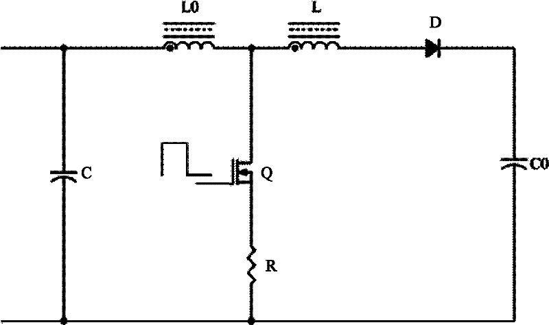
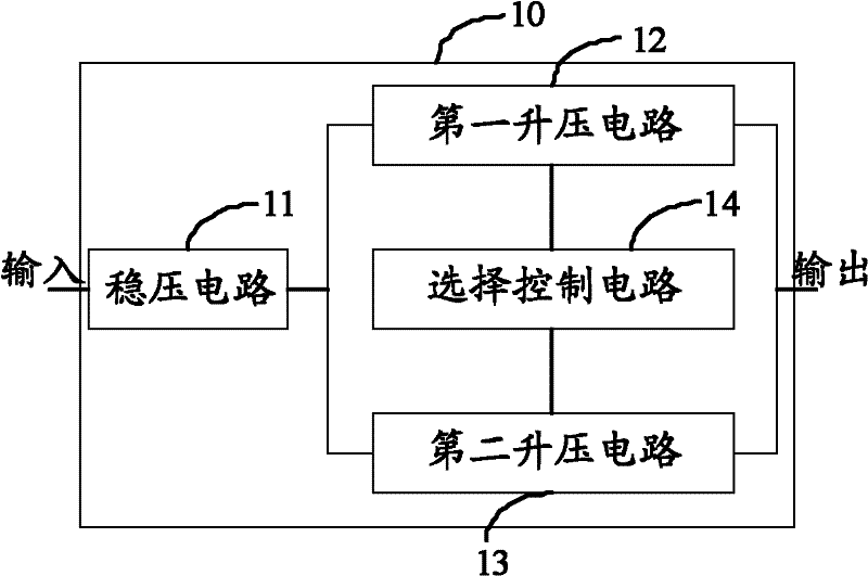
[0031] refer to figure 2 , the present invention proposes an embodiment of an LED backlight driving circuit 10 . The LED backlight driving circuit 10 supplies power for the LED backlight module (not shown), and it includes: a voltage stabilizing circuit 11, a first voltage boosting circuit 12, a second voltage boosting circuit 13 and a selection control circuit 14; the voltage stabilizing circuit 11. Receive an input voltage, filter the input voltage, and output a regulated DC power; the first boost circuit 12 receives the regulated DC power, boosts it and outputs it to the LED backlight module; the second boost circuit The circuit 13 receives the regulated direct current, boosts it and outputs it to the LED backlight module; the selection control circuit 14 alternately selects the first boost circuit 12 and the sec...
PUM
 Abstract
Description
Claims
Application Information