

Cutting edge positioning type welding structure and method for preventing pin offset
A welding structure, positioning technology, applied in the direction of printed circuits, electrical components, electrical components connected with non-printed electrical components, can solve problems such as reducing process efficiency, problems, increasing manufacturing costs, etc., to improve process efficiency, The effect of reducing manufacturing costs
- Summary
- Abstract
- Description
- Claims
- Application Information
AI Technical Summary
Problems solved by technology
Method used
Image

Examples
Embodiment Construction
[0034] In order to fully understand the purpose, features and effects of the present invention, now through the following specific embodiments, and in conjunction with the accompanying drawings, the present invention is described in detail, as follows:
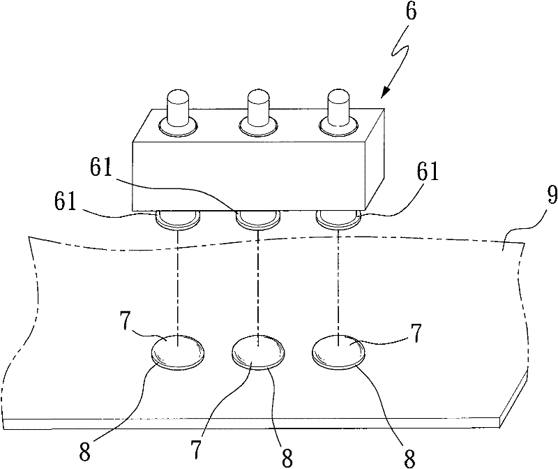
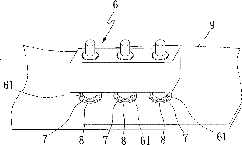
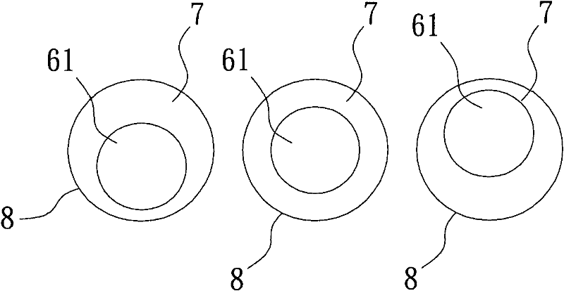
[0035] Figure 4 to Figure 6 They are respectively an exploded view, an assembled view and a top view of pins, solder and welding pads of a preferred embodiment of the present invention. As shown in the figure, the first aspect of the present invention is a trimming positioning type welding structure, including A welding pad 3 provided on the circuit board 5 is used to join the SMT electronic assembly 1 with a plurality of pins 11, the size of the welding pad 3 is larger than the pins 11, and the shape of the above-mentioned pins 11 can be circular and The number can be two or more. In the drawings, three pins 11 are taken as an example. The number of the above-mentioned welding pads 3 corresponds to the number of the above-me...
PUM
 Abstract
Description
Claims
Application Information