

Circuit board structure
A circuit board and circuit technology, applied in printed circuits, printed circuits, printed circuit manufacturing, etc., can solve the problems of numerous and complex process steps, and difficult to remove the residues of the patterned photoresist layer, so as to improve the process yield, The effect of simplifying process steps and improving process efficiency
- Summary
- Abstract
- Description
- Claims
- Application Information
AI Technical Summary
Problems solved by technology
Method used
Image

Examples
Embodiment Construction
[0037] The aforementioned and other technical contents, features and effects of the present invention will be clearly presented in the following detailed description of the embodiments with reference to the accompanying drawings. The directional terms mentioned in the following embodiments, such as: "upper", "lower", "front", "rear", "left", "right", etc., are only referring to the directions of the accompanying drawings. Accordingly, the directional terms used are illustrative, not limiting, of the invention. Also, in the following embodiments, the same or similar components will use the same or similar symbols.
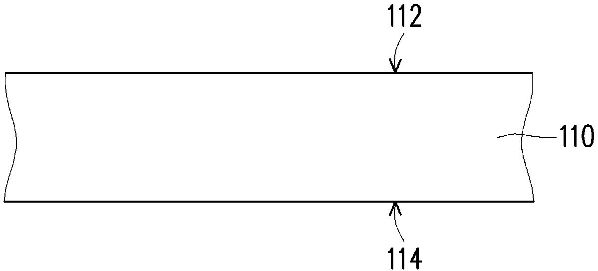
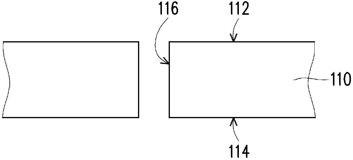
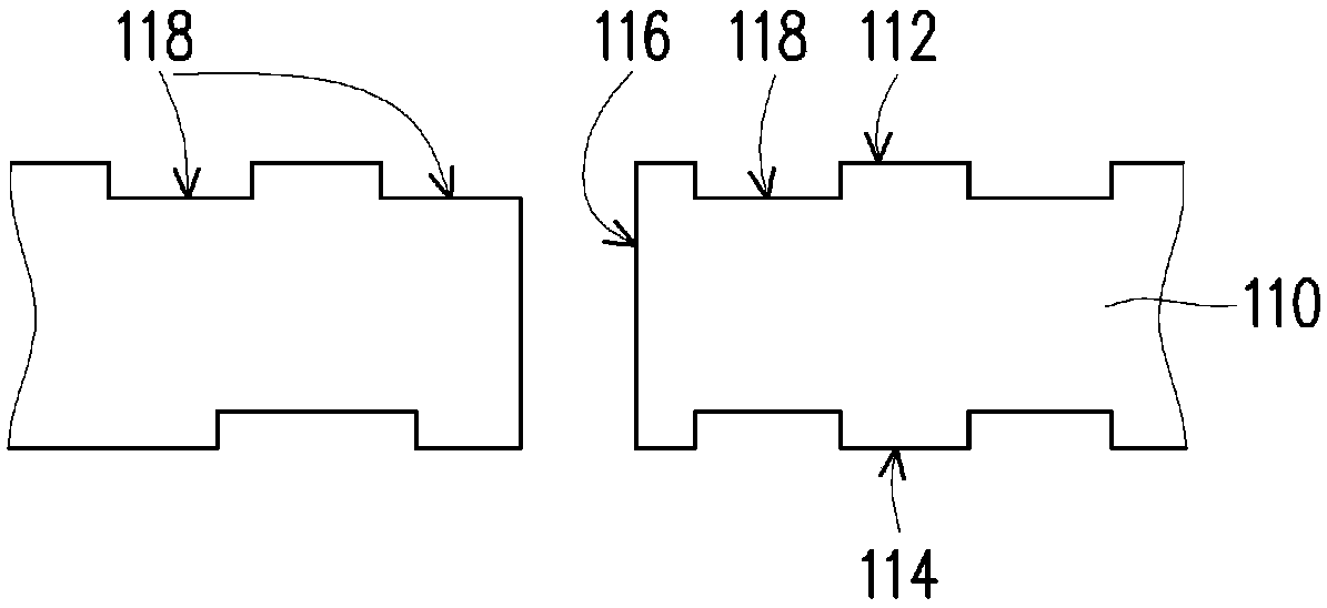
[0038] Figure 1A to Figure 1G is a schematic diagram of a circuit board structure according to an embodiment of the present invention. The manufacturing method of the circuit board structure in this embodiment may include the following steps. First, please refer to Figure 1A , providing a first metallizable insulating substrate 110 comprising an upper surface 1...
PUM
 Abstract
Description
Claims
Application Information