X-ray image sensor and method for fabricating the same

a technology fabricated parts, which is applied in the field of x-ray image sensor, can solve the problems of undesired image, adversely affecting the switching of tft 3, and increasing off-state leakage current, so as to reduce processing errors, improve yield, and simplify processing steps

Inactive Publication Date: 2002-07-23
LG DISPLAY CO LTD
View PDF7 Cites 42 Cited by
  • Summary
  • Abstract
  • Description
  • Claims
  • Application Information

AI Technical Summary

Benefits of technology

An object of the present invention is to provide an X-ray image sensor having simpler processing steps while forming a first data contact hole, a semiconductor layer, and an island-shaped semiconductor layer.
Another object of the present invention is to provide an X-ray image sensor having improved yields.
A further object of the invention is to provide a method of forming an X-ray image sensor which can reduce processing error during production by reducing mis-alignment.

Problems solved by technology

This adversely affects the switching of the TFT 3 and increases the OFF state leakage current.
Such can result in an undesired image.

Method used


Image

  • X-ray image sensor and method for fabricating the same
  • X-ray image sensor and method for fabricating the same
  • X-ray image sensor and method for fabricating the same

Examples


Embodiment Construction

Reference will now be made in detail to an illustrated embodiment of the present invention, the example of which is shown in the accompanying drawings.

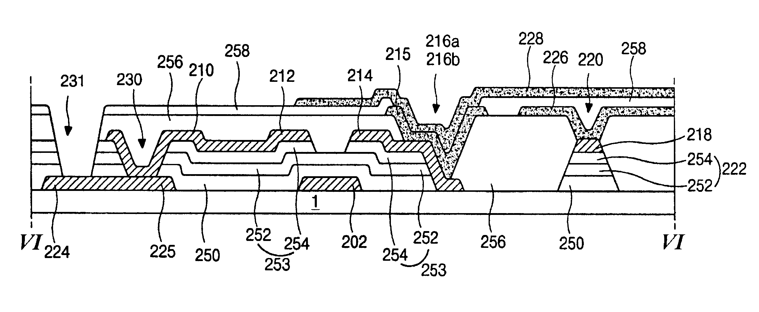
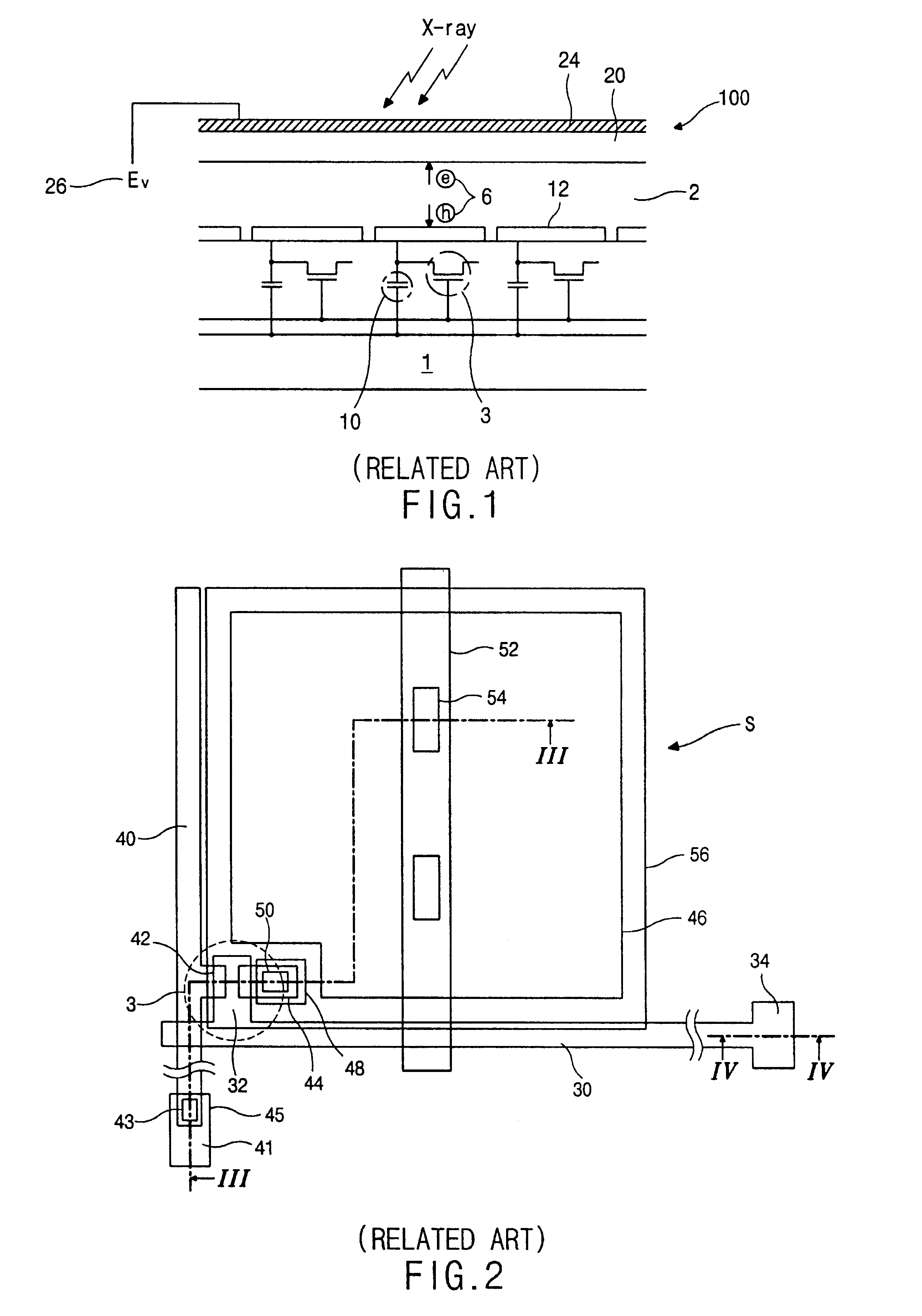
FIG. 5 is a plan view of an X-ray image sensor according to an embodiment of the present invention and is similar to the plan view of conventional X-ray image sensor (see FIG. 2).

Shown are a TFT "T", a storage capacitor "C," and gate and data lines 200 and 210. The gate line 200 is arranged in a transverse direction and the data line 210 is arranged perpendicular to the gate line 200. The TFT "T" is formed near the crossing of the gate and data lines 200 and 210. The TFT "T" includes a gate electrode 202, which is formed by an elongation of the gate line 200, and a source electrode 212, which is formed by an elongation of the data line 210. The TFT "T" also includes a drain electrode 214 that is spaced apart from the source electrode 212.

A ground line 218 is arranged parallel to the data line 210 and perpendicular to the gate line 200...


PUM


Abstract

An X-ray image sensor fabricated using eight-mask steps. A thin film transistor (TFT) having a gate electrode, a first insulation layer, pure and doped amorphous silicon layers, and source and drain electrodes is on a substrate. An island-shaped first insulation layer, semiconductor layer, and ground line are also formed. A second insulation layer having a first drain contact hole and a ground line contact hole covers the TFT, the substrate, and the ground line. An auxiliary drain electrode on the second insulation layer contacts the drain electrode through the first drain contact hole. A capacitor electrode on the second insulation layer contacts the ground line through the ground line contact hole. A third insulation layer having a second drain contact hole that exposes the auxiliary drain is on the second insulation layer, the auxiliary drain electrode, and the capacitor electrode. A pixel electrode on the third insulation layer contacts the auxiliary drain electrode through the second drain contact hole.

Description

This application claims the benefit of Korean Patent Application No. 1999-67854, filed on Dec. 31, 1999, which is hereby incorporated by reference for all purposes as if fully set forth herein.BACKGROUND OF THE INVENTION1. Field of the InventionThe present invention relates to X-ray image sensors. More particularly, it relates to X-ray image sensors having a TFT (Thin Film Transistor) array, and to a method for fabricating the same.2. Discussion of the Related ArtX-ray detection has been widely used for medical diagnosis. X-ray detection typically uses an X-ray film to produce a photograph. Therefore, some predetermined developing and printing procedures are required to produce the photograph.However, digital X-ray image sensors that employ TFTs (Thin Film Transistors) have been developed. Such X-ray image sensors have the advantage that a real time diagnosis can be obtained.FIG. 1 is a schematic, cross-sectional view illustrating the structure and operation of an X-ray image sensin...

Claims


Application Information

Patent Timeline
Patent Type & Authority Patents(United States)
IPC IPC(8): G01T1/00G01T1/24H01L21/02H01L21/331H04N5/32H01L27/146
CPCH01L27/14665H01L27/14696H04N5/32
Inventor CHOO, KYO-SEOPPARK, JUNE-HO
Owner LG DISPLAY CO LTD
Why Eureka
Try Eureka