3D NAND memory and forming method thereof

A 3D NAND and memory technology, which is applied in the direction of semiconductor devices, electrical solid state devices, electrical components, etc., can solve problems affecting memory performance, and the characteristic size of gate spacers is easy to fluctuate, so as to ensure stability and improve performance.

Active Publication Date: 2019-08-09
YANGTZE MEMORY TECH CO LTD
View PDF5 Cites 41 Cited by
  • Summary
  • Abstract
  • Description
  • Claims
  • Application Information

AI Technical Summary

Problems solved by technology

[0004] Existing memories generally include several memory blocks (Blocks), and the gate spacers between the memory blocks generally pass through the stack structure in the vertical direction, and the gate spacers on both sides of the pseudo-common source are exposed. The sidewall (Gate Line Slit, GLS) corresponding to the pseudo common source is separated, but in the manufacturing process of the existing 3D NAND memory, the characteristic size of the gate spacer is easy to fluctuate, which affects the performance of the memory

Method used


Image

  • 3D NAND memory and forming method thereof
  • 3D NAND memory and forming method thereof
  • 3D NAND memory and forming method thereof

Examples


no. 1 example 3D

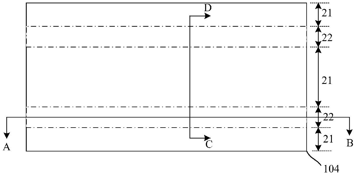
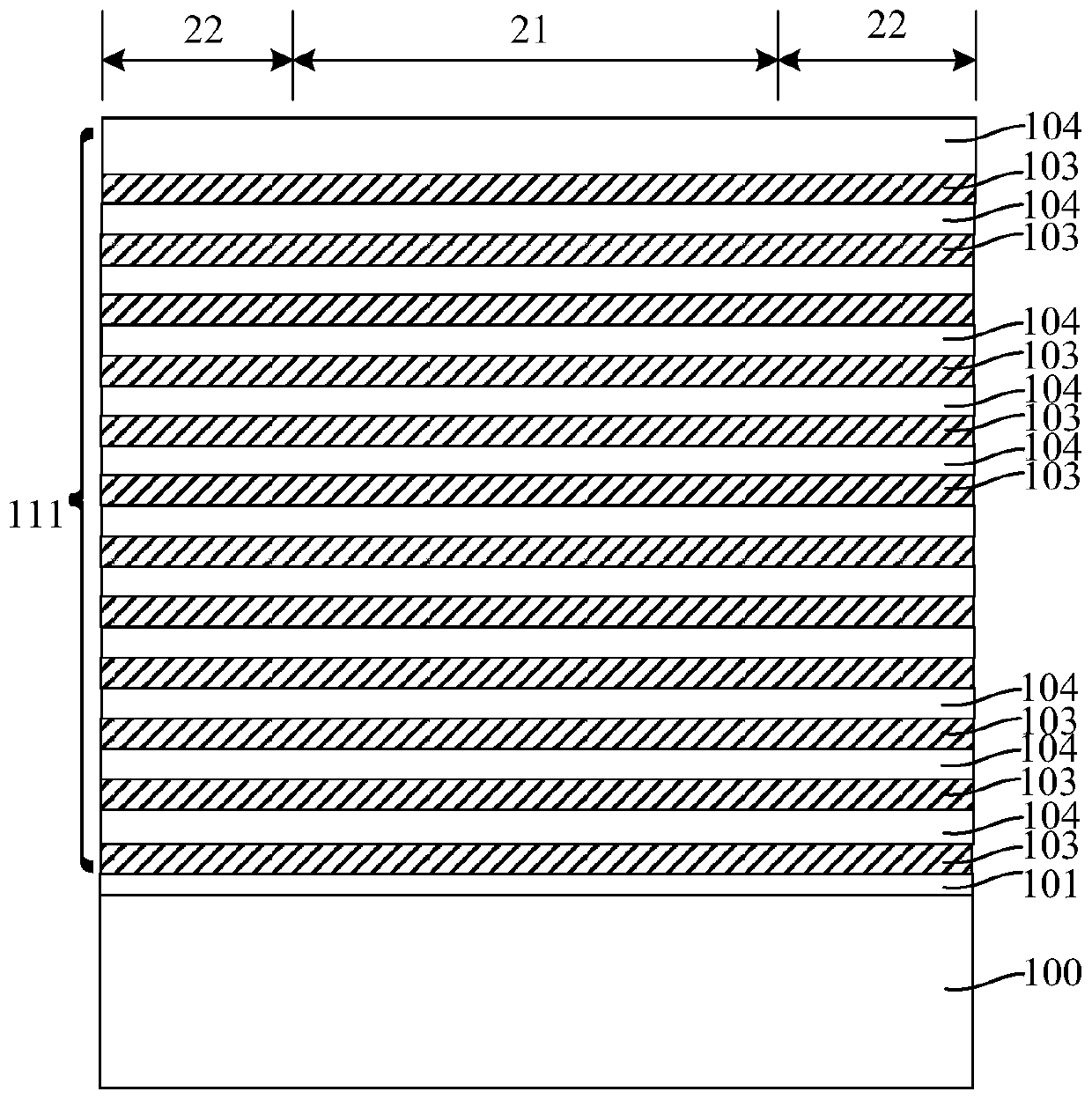
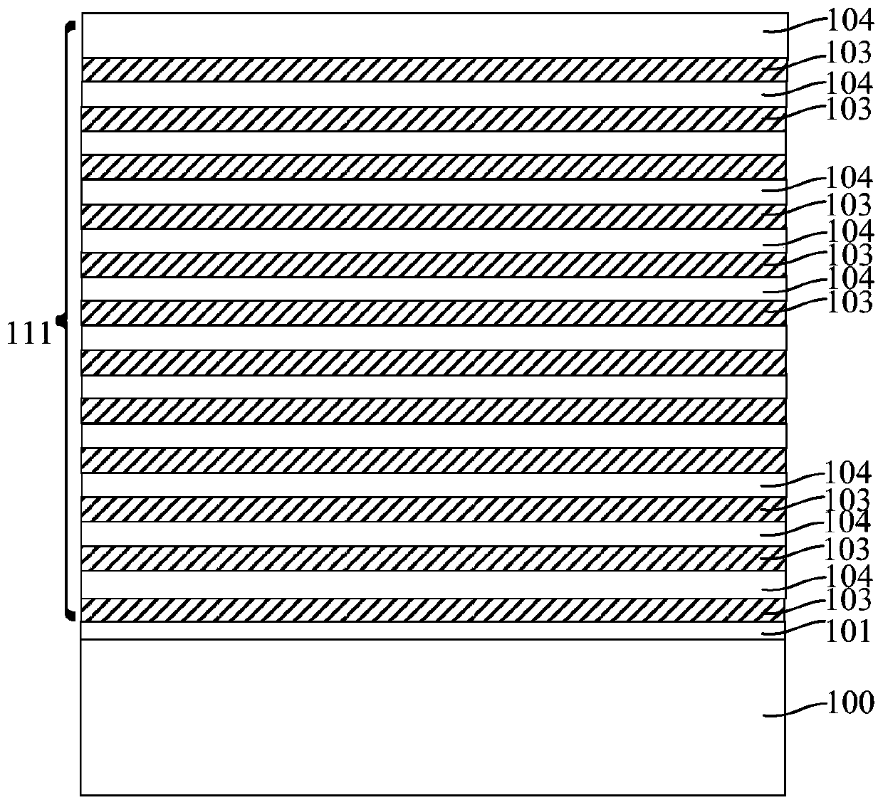
[0048] Figure 1-Figure 21 It is a structural schematic diagram of the 3D NAND formation process according to the first embodiment of the present invention.

[0049] refer to Figure 1-Figure 3 , figure 2 for figure 1 A schematic cross-sectional view along the cutting line AB, image 3 for figure 1 A schematic cross-sectional structure along the cutting line CD, providing a semiconductor substrate 100, on which a stacked structure 111 in which sacrificial layers 103 and isolation layers 104 are alternately stacked is formed, and the stacked structure 111 includes several parallel gates The spacer region 22 , and the through hole region 21 is formed between adjacent gate spacer regions 22 .

[0050] The material of the semiconductor substrate 100 can be single crystal silicon (Si), single crystal germanium (Ge), or silicon germanium (GeSi), silicon carbide (SiC); it can also be silicon on insulator (SOI), germanium on insulator (GOI); or other materials, such as III-V g...


PUM


Abstract

A 3D NAND memory and a forming method thereof are disclosed. According to the forming method of the 3D NAND memory, at least one pseudo common source penetrating a stacking structure is formed in gateisolation groove regions, gate isolation grooves penetrating the stacking structure are subsequently formed in the gate isolation groove regions on the two sides of the pseudo common sources, and thegate isolation grooves formed on the two sides of the pseudo common sources expose the corresponding side walls of the pseudo common sources. In the process of forming the gate isolation grooves, inthe process of removing a sacrificial layer after the formation of the gate isolation grooves and in the process of forming control gates and array common sources, the pseudo common sources can support the two side walls of the gate isolation grooves and prevent the two side walls of the gate isolation grooves from deforming or tilting. Thus, the stability of the characteristic dimensions of the formed gate isolation grooves is ensured, and the performance of the 3D NAND memory is improved.

Description

technical field [0001] The invention relates to the field of semiconductor manufacturing, in particular to a method for reducing 3D NAND memory. Background technique [0002] NAND flash memory is a non-volatile storage product with low power consumption, light weight and good performance, and has been widely used in electronic products. At present, the NAND flash memory with a planar structure is close to the limit of practical expansion. In order to further increase the storage capacity and reduce the storage cost per bit, a 3D NAND memory with a 3D structure is proposed. [0003] The formation process of the existing 3D NAND memory generally includes: forming a stacked structure in which isolation layers and sacrificial layers are alternately stacked on the substrate; etching the stacked structure, forming channel vias in the stacked structure, and forming channel vias Finally, etch the substrate at the bottom of the channel via hole to form a groove in the substrate; in ...

Claims


Application Information

Patent Timeline
Patent Type & Authority Applications(China)
IPC IPC(8): H01L27/11524H01L27/11556H01L27/1157H01L27/11582
CPCH10B41/35H10B41/27H10B43/35H10B43/27H10B43/10
Inventor 霍宗亮欧文杨号号徐伟严萍黄攀周文斌
Owner YANGTZE MEMORY TECH CO LTD
Why Eureka
Try Eureka