Apparatus for producing Ic chip mounter

A technology for manufacturing devices and chip mounting, which is applied to record carriers, instruments, computer parts, etc. used in machines. It can solve the problems of damage, prolong the total length of the heating and pressurizing mechanism, weak impact ability, etc., and reduce friction. coefficient, improve yield, and prevent damage

Inactive Publication Date: 2012-01-04
SHINKO ELECTRIC CO LTD
View PDF6 Cites 2 Cited by
  • Summary
  • Abstract
  • Description
  • Claims
  • Application Information

AI Technical Summary

Problems solved by technology

[0007] However, in the manufacturing apparatus of the above-mentioned IC chip package, while continuously conveying the substrate or the film substrate, sticking the circuit chip, loading the IC chip, and performing thermocompression bonding in order to cure the adhesive, it is also necessary to For quite a long time, it is necessary to extend the total length of the heated and pressurized mechanism part, which requires a lot of space
In addition, the IC chip is a very fine (for example, less than 1 mm square) precision component, and its ability to withstand external pressure and impact is very weak. Therefore, it is considered that when the adhesive is cured, once the IC chip is subjected to excessive pressure, it will be damaged. The possibility of damage may lead to a decrease in the yield of the IC chip package
Moreover, it is also difficult to adjust the pressure to the extent that the IC chip will not be damaged
In view of the above-mentioned various reasons, in the conventional IC chip package manufacturing equipment, there will be waste in terms of time, cost, space, and yield.

Method used


Image

  • Apparatus for producing Ic chip mounter
  • Apparatus for producing Ic chip mounter
  • Apparatus for producing Ic chip mounter

Examples


Embodiment Construction

[0030] Hereinafter, an embodiment of the present invention will be described with reference to the drawings.

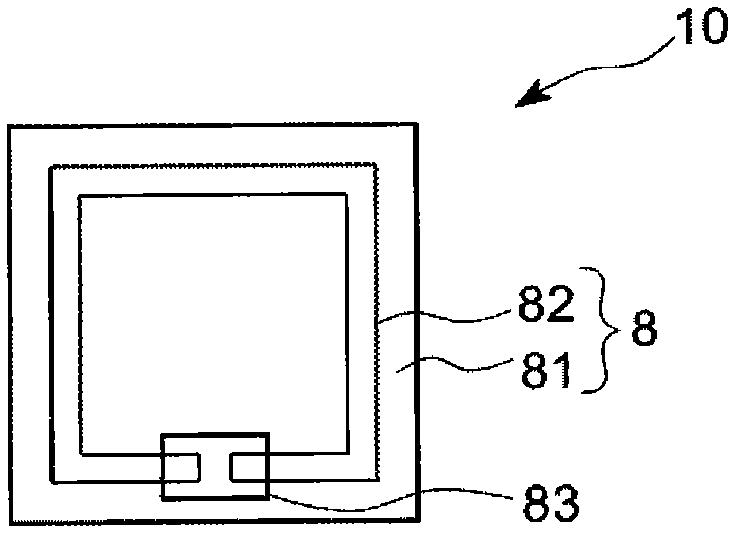
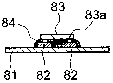
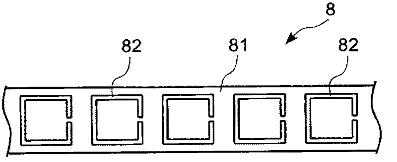
[0031]First, the IC tag 10 which is an example of the IC chip package manufactured by the manufacturing apparatus of the IC chip package of this invention is demonstrated. figure 1 It means from the IC chip package 9 (refer to Figure 4 ) is a top view of an IC tag 10 cut out, figure 2 is a schematic diagram showing a longitudinal cross-sectional view of the IC tag. The antenna circuit 82 is preformed on the substrate 81 by printing and etching, such as image 3 As shown, a plurality of antenna circuits 82 are continuously formed on the substrate 81 at intervals (for example, at equal intervals). The IC tag 10 includes a thin film substrate 8 and an IC chip 83, the thin film substrate 8 is formed with an antenna circuit 82 at a predetermined position on one surface of the substrate 81; load. Figure 4 It is a top view schematically showing the sheet-shaped IC ch...


PUM


Abstract

Provided is an IC chip mounter production apparatus which can allow curing of an adhesive for a short time without requiring a large space for a heating and pressurizing mechanism for the adhesive to secure an IC chip on a film substrate, and rarely damages IC chips to increase the yield. The IC chip mounter production apparatus (1) is configured in a manner that a carrying passage for a film substrate (8) on which an antenna circuit (82) is formed and an IC chip (83) is mounted through an adhesive (84), is provided with a thermal compression part (5) wherein a cover sheet (85) is laid on the film substrate (8) to cover the same and the IC chip (83) is bonded on the film substrate (8) by thermal compression, and a cover sheet supply part (4); and the thermal compression part (5) comprises a belt (82) to hold the film substrate (8) mounted with the IC chip (83) between the belt and the cover sheet (85), a tensile force providing means (84a) to provide a tensile force to the cover sheet (85), and a heating means (86) to heat the film substrate (8).

Description

technical field [0001] The present invention relates to a manufacturing device of an IC chip package. Background technique [0002] In recent years, a wireless IC tag, which is a type of RFID (Radio Frequency Identification, radio frequency identification), has been used as a package on which an IC chip is mounted. Among IC tags, a tag called a passive electronic tag (Passive tag) has a structure that does not load a battery, and an IC chip with unique identification information and a small antenna circuit are pasted on a film substrate. The electric wave sent by the reader generates a small amount of power inside the circuit, and uses this power to communicate with the IC tag reader to read and write the information in the IC chip. As a non-contact IC card, it can be used in bus cards, electronic money, authentication cards, etc. widely used in the field. In addition, recently, an IC chip called an active tag (Active tag) that is equipped with a battery and emits radio wa...

Claims


Application Information

Patent Timeline
Patent Type & Authority Applications(China)
IPC IPC(8): G06K19/077G06K19/07
CPCG06K19/07718G06K19/077
Inventor 森田将司井上太一松屋千春谷井正和
Owner SHINKO ELECTRIC CO LTD
Why Eureka
Try Eureka