
Mask plate and mask plate manufacturing method

A manufacturing method and mask plate technology, applied in the field of mask plate and mask plate production in photolithography technology, to achieve the effects of increasing data collection, improving production efficiency, and reducing the number of repeated exposures

Active Publication Date: 2013-04-10
SHANGHAI MICRO ELECTRONICS EQUIP (GRP) CO LTD
View PDF0 Cites 2 Cited by
  • Summary
  • Abstract
  • Description
  • Claims
  • Application Information

AI Technical Summary

Problems solved by technology

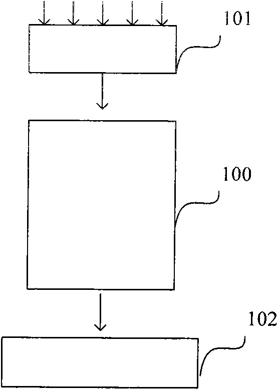
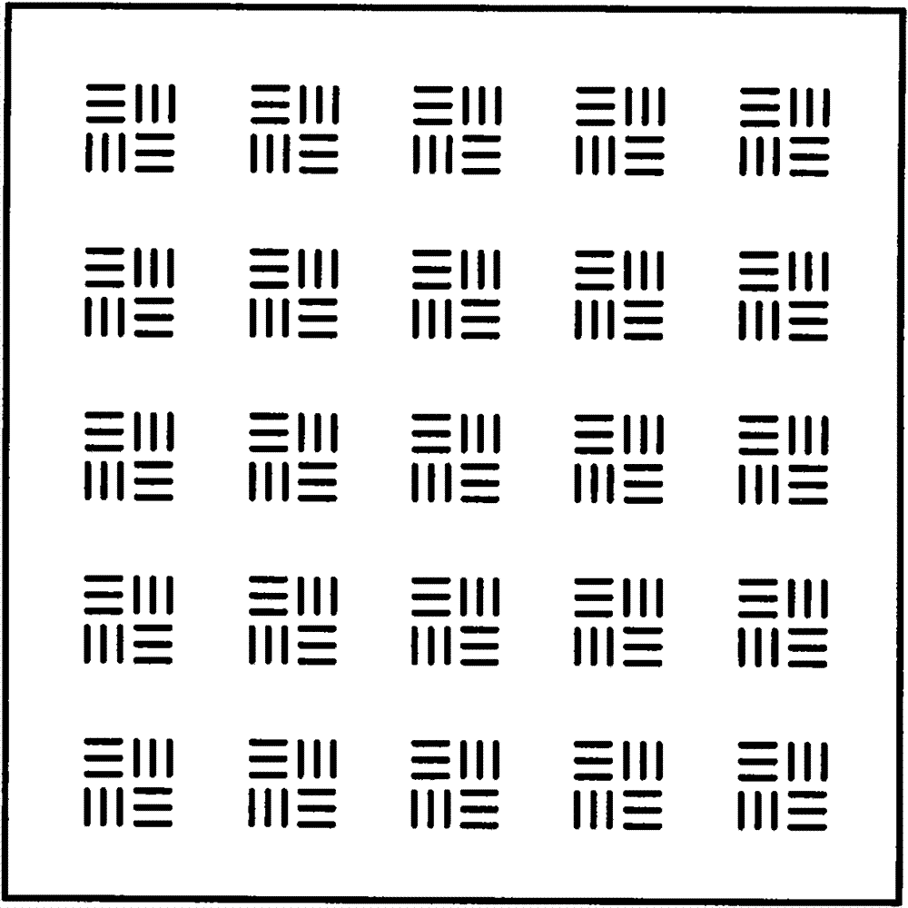
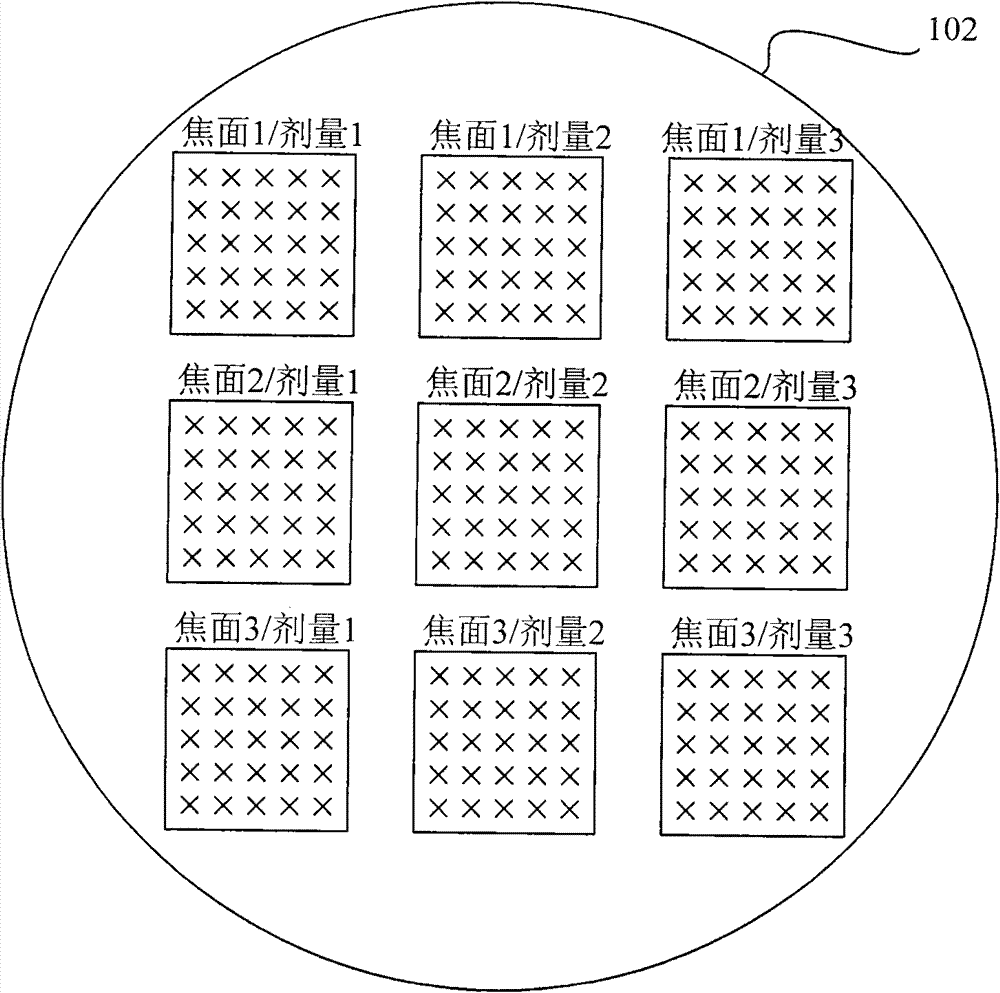
[0008] The technical problem solved by the present invention is that under the condition of single exposure, the existing reticle can only obtain the image pattern corresponding to a single exposure dose and a single object distance

Method used


Image

  • Mask plate and mask plate manufacturing method
  • Mask plate and mask plate manufacturing method
  • Mask plate and mask plate manufacturing method

Examples


Embodiment Construction

[0050] refer to Figure 4 , the present invention provides a reticle 300 suitable for mask exposure testing. Specifically, the reticle 300 includes: a substrate 301, a plurality of mask components 302 with different thicknesses located on one side of the substrate 301, the surface of the mask components 302 has mask marks 304; The filter film 303.

[0051] The implementation of the present invention will be further described in detail below in conjunction with the drawings and specific embodiments.

[0052] In a specific embodiment, refer to Figure 5, the filter film 303 and the mask part 302 including the mask marks 304 are respectively located on two sides of the substrate 301 . For example, the filter film 303 can be arranged on the surface of the substrate 301 on the light-incident side, and the mask component 302 comprising the mask mark 304 can be arranged on the surface of the substrate 301 on the light-emitting side, wherein the mask mark 304 is located at the same...


PUM


Abstract

The invention relates to a mask plate and a mask plate manufacturing method. The mask plate comprises a substrate, a plurality of mask components and a filter film, wherein the mask components are arranged on one side of the substrate and have different thicknesses, the surfaces of the mask components are provided with mask markers, and the mask markers are arranged on the surfaces of the mask components for light transmission during exposure; and the filter film covers the substrate and has a plurality of light transmission rates. Since the mask components with the mask markers are arranged corresponding to multiple light transmission rates, image patterns corresponding to multiple mask markers with different object distances and different light intensities can be obtained in a single exposure, the number of repeated exposures can be reduced, and the production efficiency can be increased.

Description

technical field [0001] The invention relates to photolithography process technology, in particular to a mask plate and a mask plate manufacturing method in the photolithography technology. Background technique [0002] With the development of integrated circuits, the design size is getting smaller and smaller, and the deformation and deviation between the photolithography pattern and the mask pattern actually obtained on the wafer will directly affect the circuit performance and production yield. [0003] Photolithography is a common process for transferring design patterns onto wafers. Generally speaking, the photolithography process includes: illuminating the mask plate through the illumination system, receiving the outgoing light through the projection objective lens, and projecting it onto the photoresist on the wafer surface, and then, through subsequent steps such as development and etching, to realize Transfer the mask pattern onto the photoresist on the wafer surfac...

Claims


Application Information

Patent Timeline
Patent Type & Authority Patents(China)
IPC IPC(8): G03F1/44G03F1/38G03F7/20
Inventor 江传亮杨志勇
Owner SHANGHAI MICRO ELECTRONICS EQUIP (GRP) CO LTD
Learn More