
Device-matched IC (integrated circuit) and design method thereof

A technology of integrated circuits and design methods, applied in CAD circuit design, circuits, electrical solid devices, etc., can solve the problems that the resistors cannot be arranged in the same center of mass, and the resistors cannot be accurately matched, etc., to achieve easy wiring, solve wiring problems, The effect of reducing production costs

Active Publication Date: 2012-02-01
SILERGY SEMICON TECH (HANGZHOU) CO LTD
View PDF3 Cites 0 Cited by
  • Summary
  • Abstract
  • Description
  • Claims
  • Application Information

AI Technical Summary

Problems solved by technology

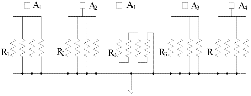
However, with such a matching method, the resistors to be matched cannot be arranged at the same centroid. When the lithography environment of each resistor is inconsistent, there are doping concentration gradients, thermal distribution gradients, stress gradients and other factors, all of which will cause the resistors to fail. exact match

Method used


Image

  • Device-matched IC (integrated circuit) and design method thereof
  • Device-matched IC (integrated circuit) and design method thereof
  • Device-matched IC (integrated circuit) and design method thereof

Examples


Embodiment Construction

[0042] Several preferred embodiments of the present invention will be described in detail below with reference to the accompanying drawings, but the present invention is not limited to these embodiments. The present invention covers any alternatives, modifications, equivalent methods and schemes made on the spirit and scope of the present invention. In order to provide the public with a thorough understanding of the present invention, specific details are set forth in the following preferred embodiments of the present invention, but those skilled in the art can fully understand the present invention without the description of these details.

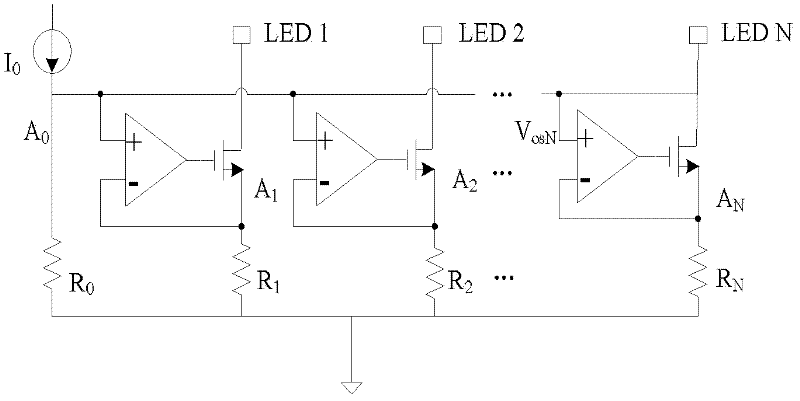
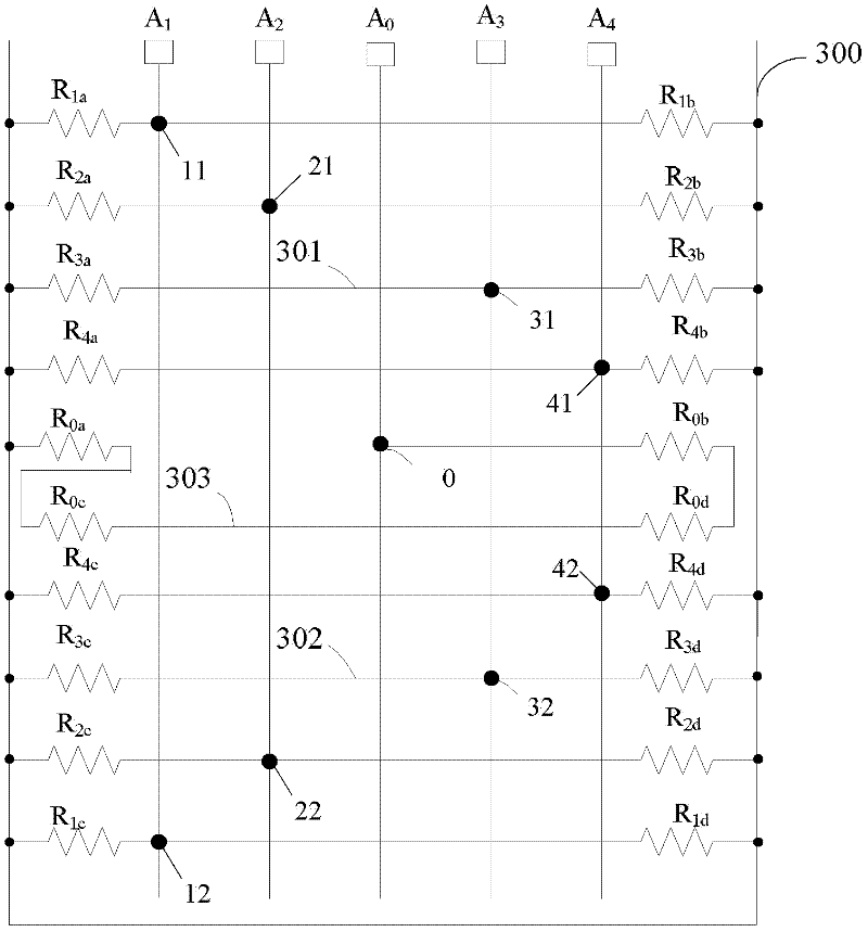
[0043] The device-matching integrated circuit provided by the embodiment of the present application includes N devices to be matched, N metal lead-out lines and a common connection line, wherein, please refer to image 3 ,show figure 1 The structure diagram of the first embodiment of the integrated circuit corresponding to the device match...


PUM


Abstract

The invention provides a device-matched IC (integrated circuit) and a design method thereof. The method comprises the following steps of: classifying devices required to be matched into unit devices with a certain number; using a mirror image method to distribute the unit devices in a form of having a shared mass center; and connecting the unit devices by metal outgoing lines, metal connecting lines and through holes between the metal outgoing lines and the connecting lines, thus reducing influences of the doping density gradient, the thermal diffusion gradient, the stress gradient and the like on device matching degree and overcoming the defects in the traditional method. In addition, through holes are distributed in the approximate shared mass center mode, so that parasitic resistances on the metal lines can be matched mutually, thus improving the matching accuracy further; and connection modes of common ports of the devices are improved, thus the layout area is saved further. Moreover, the design method of the device-matched IC is suitable for various devices and has no limit on the number of the devices; and in the design method, the two layers of metal lines are used only forthe connection of the unit devices, the arrangement of the lines is easier, and the production cost is reduced.

Description

technical field [0001] The invention relates to the field of integrated circuit design, in particular to an integrated circuit for device matching and a design method thereof. Background technique [0002] In the layout design of integrated circuits, device matching has always been an important issue we pay attention to. Such as figure 1 As shown, it is a typical multi-channel LED drive circuit that requires high matching of devices. exist figure 1 In the circuit shown, current matching between channels is critical. which flows through the resistor R o current I o It is set externally by the user, and the current of each LED channel is shown in formula (1): [0003] I LED - N = I o R 0 + V osN ...

Claims


Application Information

Patent Timeline
Patent Type & Authority Applications(China)
IPC IPC(8): H01L27/02G06F17/50
CPCG06F17/50H01L27/0802H01L27/0207G06F17/5045G06F30/30
Inventor 程帅
Owner SILERGY SEMICON TECH (HANGZHOU) CO LTD
Learn More