Method for detecting appearance of semiconductor chip

An appearance inspection and chip technology, which is applied to measurement devices, optical devices, optical testing of flaws/defects, etc., can solve the problems of high cost and complex structure of inspection devices, and achieve the effects of compact structure, uniform lighting and high contrast.

Active Publication Date: 2012-02-22
HUAZHONG UNIV OF SCI & TECH
View PDF2 Cites 50 Cited by
  • Summary
  • Abstract
  • Description
  • Claims
  • Application Information

AI Technical Summary

Problems solved by technology

[0006] At present, the structure of the appearance inspection system based on machine vision is relatively complicated, and the cost of the inspection device is high

Method used


Image

  • Method for detecting appearance of semiconductor chip
  • Method for detecting appearance of semiconductor chip
  • Method for detecting appearance of semiconductor chip

Examples


Embodiment Construction

[0030] The present invention will be described in further detail below in conjunction with the accompanying drawings and specific embodiments.

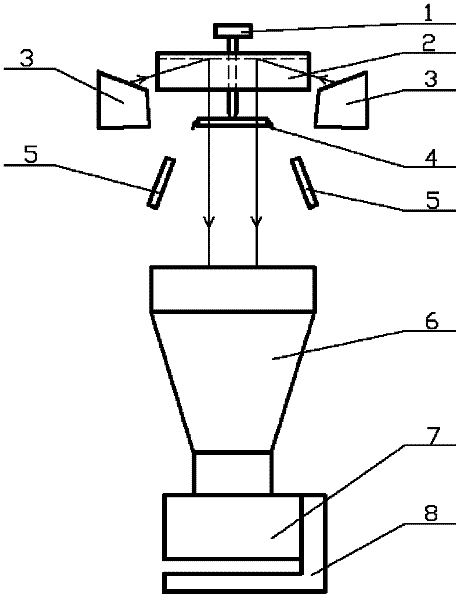
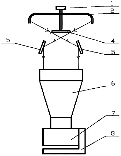
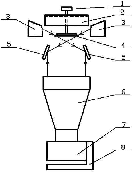
[0031] like figure 1 , The appearance inspection device of the semiconductor chip of the present invention includes a suction mechanism 1, a U-shaped reflector 2, two light sources 3, four plane mirrors 5, a lens 6, a camera 7 and a working distance adjustment mechanism 8.

[0032] The suction mechanism 1 is responsible for sucking the device 4 to be tested to the detection position. After the detection is completed, the suction device 1 leaves the detection position; the U-shaped reflector 2 is installed on the suction mechanism 1 to reflect light. The specific principle is that the light emitted by the light source 3 is irradiated on the U-shaped reflector 2, and is reflected by the U-shaped reflector 2. Figure 11 The device side 1 and side 3 or side 2 and side 4) in the device are backlit, and move together with the suction mecha...


PUM


Abstract

The invention discloses a method for detecting appearance of a semiconductor chip. The device comprises a sucking mechanism, a U-shaped reflecting plate, two light sources, plane reflecting mirrors, a lens, a camera and an adjusting mechanism, wherein the sucking mechanism is used for sucking a chip to be detected to a position to be detected; the U-shaped reflecting plate is arranged on the sucking mechanism; the two light sources are symmetrically arranged on the side of the chip; one part of light emitted by the two light sources irradiates the U-shaped reflecting plate and performs backlight illumination on the bottom surface and one group of opposite sides of the chip, and the other part of light performs backlight illumination on the other group of opposite sides of the chip; a plurality of plane reflecting mirrors are obliquely and symmetrically arranged at the periphery below the chip, so that light rays reflected by the plane reflecting mirrors are vertically transmitted to the front end face of the lens; the lens is arranged on the camera and positioned below the chip; the camera is arranged on the adjusting mechanism; and the adjusting mechanism is used for adjusting the working distance of the camera. By a backlight illumination technology, a device is clearly imaged, contrast is high, lighting uniformity is achieved, detection time is shortened, and efficiency is improved.

Description

technical field [0001] The present invention relates to the field of optical detection devices, in particular to a detection device for semiconductor integrated circuit chips, which is mainly applied to (but not limited to) semiconductor chips of square flat packaging technology, and can detect missing or damaged pins of the chip. , pin width, pin spacing, pin length deviation, pin stack height, pin coplanarity, pin bending, pin span, pin row bending, pin tilt and other indicators are tested. Background technique [0002] In the semiconductor industry, before the packaged integrated circuit device is used as a patch component, it needs to go through an effective pin appearance inspection. The inspection items generally include pin spacing, width, span, and stack height. In large-scale production, the following methods are traditionally used to inspect the appearance of device tube legs: make limit samples of various appearance items in advance, compare the actual devices tha...

Claims


Application Information

Patent Timeline
Patent Type & Authority Applications(China)
IPC IPC(8): G01B11/00G01N21/88
Inventor 王瑜辉尹周平熊有伦罗明成张少华
Owner HUAZHONG UNIV OF SCI & TECH
Why Eureka
Try Eureka