Wiring structure of touch panel and manufacturing method thereof

A wiring structure and touch panel technology, applied in the input/output process of data processing, instruments, electrical digital data processing, etc., can solve the problems of high equipment power, high operating cost, and large resource consumption, and achieve equipment power low effect

Inactive Publication Date: 2012-03-14
利信光学(苏州)有限公司
View PDF3 Cites 5 Cited by
  • Summary
  • Abstract
  • Description
  • Claims
  • Application Information

AI Technical Summary

Problems solved by technology

[0003] 1. The thinnest line width of printing has limitations, and the ultra-fine line processing of products cannot be carried out, and the design of narrow edge products cannot be carried out;
[0004] 2. Wet engraved line body maintenance items consume more resources, manpower and material resources, and the cost is relatively high;
[0005] 3. There are many production links; the production yield and efficiency are relatively low;
[0006] 4. The operation requires acid and alkali liquid, pure water, relatively high equipment power, high overall operating cost, and is not environmentally friendly

Method used


Image

  • Wiring structure of touch panel and manufacturing method thereof
  • Wiring structure of touch panel and manufacturing method thereof

Examples


Embodiment Construction

[0025] In the following, the specific implementation manners of the present invention will be further described in detail in conjunction with the accompanying drawings of the embodiments, so as to make the technical solution of the present invention easier to understand and grasp.

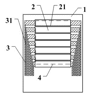
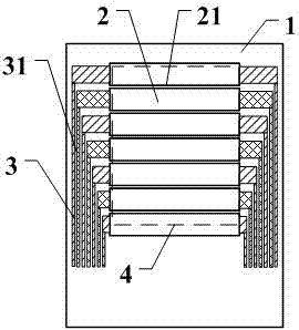
[0026] like figure 1 As shown, it is a schematic diagram of a specific touch panel wiring structure. It can be seen from the figure that the touch panel includes a substrate 1 and a transparent conductive film 2 coated thereon, wherein the transparent conductive film covers at least the entire substrate. The functional area 4, and the transfer line 3 is arranged on the substrate through the functional area. In order to realize the touch function, the transparent conductive film 2 is provided with a plurality of dividing lines 21 in the functional area corresponding to each line of the transfer line low-resistance conductive film, wherein the minimum line width of the dividing line is 10 μm, and the...


PUM


Abstract

The invention discloses a wiring structure of a touch panel and a manufacturing method thereof. The wiring structure comprises a substrate, a transparent conductive film which covers the substrate and the whole functional region and a switching line which is arranged in a way of penetrating the functional region of the substrate, wherein the switching line is a low-resistance conductive film in a line structure, the transparent conductive film is provided with a plurality of split lines corresponding to the switching circuit in the functional region. The wiring structure is characterized in that the minimum line width of the spit lines is 10mum, intervals of the lines of the switching line, which are arranged at the periphery of the functional region of the substrate, range from 10mum to 200mum. The manufacturing method comprises the steps of splitting the transparent conductive film and the low-resistance conductive film by adopting certain laser power and laser length and etching among the lines of the switching line, which are arranged at the periphery of the functional region so as to reserve the transparent and low-resistance conductive films on the surface of the lines. By applying the technical scheme in the invention, narrow side design of a product can be realized, stability and reliability of the product can be improved, operating processes and operating personnel are reduced, cost is reduced, energy is saved while waste is reduced, and production efficiency and processing yield are increased.

Description

technical field [0001] The invention relates to a structure of a touch panel, in particular to a wiring structure and a manufacturing method thereof for corresponding touch sense and transmission of control signals on the touch panel. Background technique [0002] With the popularization and rapid development of portable electronic information interactive devices, the traditional hard keyboard has quietly disappeared, and the touch operation based on the display interface is the mainstream. More and more technicians are devoting themselves to the research of the touch panel, and the control recognition accuracy, product stability and reliability, and product manufacturing efficiency of the touch panel are the main research focuses. In order to make the ratio of the functional area used for display to the wiring area for line transmission larger and larger when the size of the touch panel is constant, designers are trying their best to reduce the line width while the circuit ...

Claims


Application Information

Patent Timeline
Patent Type & Authority Applications(China)
IPC IPC(8): G06F3/041
Inventor 黄良杰杜秀兰陈伟
Owner 利信光学(苏州)有限公司
Why Eureka
Try Eureka