camera device

一种摄像装置、摄像部的技术,应用在图像通信、电视、彩色电视的零部件等方向,能够解决损害摄像图像画质等问题

Active Publication Date: 2017-11-21
NIKON CORP
View PDF1 Cites 0 Cited by
  • Summary
  • Abstract
  • Description
  • Claims
  • Application Information

AI Technical Summary

Problems solved by technology

[0003] However, in order to shorten the acquisition time of correction data, a method of acquiring correction data only from a part of lines in one screen is adopted. In this case, pixel amplifiers of the lines for which correction data Since pixel amplifiers have different operating points, when used in an area where the input and output characteristics of the pixel amplifier are non-linear, there is a problem that the signal level between lines will vary, which may impair the image quality of the captured image.

Method used


Image

  • camera device
  • camera device
  • camera device

Examples


Embodiment Construction

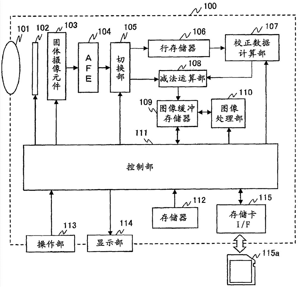
[0023] Hereinafter, embodiments of the imaging device of the present invention will be described in detail using the drawings. figure 1 It is a block diagram showing the structure of the electronic video camera 100 corresponding to the imaging device of the present invention.

[0024] (Structure of electronic camera 100)

[0025] exist figure 1 Among them, the electronic camera 100 is composed of an optical system 101, a mechanical shutter 102, a solid-state imaging element 103, an AFE (analog front end) 104, a switching unit 105, a line memory 106, a correction data calculation unit 107, a subtraction unit 108, an image buffer memory 109, An image processing unit 110 , a control unit 111 , a memory 112 , an operation unit 113 , a display unit 114 , and a memory card I / F 115 are configured.

[0026] The optical system 101 forms an image of light input from a subject on the light receiving surface of the solid-state imaging device 103 .

[0027] The mechanical shutter 102 is...


PUM


Abstract

The present invention provides an imaging device, which includes an imaging unit and a correction unit. The imaging unit is composed of a pixel array and a readout control unit. A plurality of pixels are arranged in a matrix in the pixel array. A transfer transistor for transferring to the drift diffusion region, an amplification transistor for outputting a pixel signal corresponding to the charge stored in the drift diffusion region, and a reset transistor for resetting the charge stored in the drift diffusion region, the readout control section controls the first readout Switch with the second readout control to perform readout. The first readout control controls the reset transistor to be turned off before exposure, and reads out pixel signals from a part of the row of the pixel array. The pixel signals are read out from the array, and the correction unit corrects the pixel signals read out by the second readout control based on the pixel signals read out by the first readout control.

Description

technical field [0001] The present invention relates to imaging devices. Background technique [0002] A general electronic camera is equipped with a solid-state imaging element such as a CCD sensor or a CMOS sensor. For example, in the case of a CMOS sensor, charges accumulated by pixels arranged in a matrix on the light receiving surface in response to incident light are converted from charge to voltage by pixel amplifiers and read out to vertical signal lines for each row. And, the signal read from each pixel is read to the outside of the CMOS sensor via a column amplifier, a CDS circuit (correlated double sampling circuit), a horizontal output circuit, and an output amplifier. However, the signal read from the CMOS sensor includes noise components inherent in the row direction, such as fixed pattern noise components and dark shading components. Therefore, in order to remove these noise components, a technique of correcting image data read from the CMOS sensor after exp...

Claims


Application Information

Patent Timeline
Patent Type & Authority Patents(China)
IPC IPC(8): H04N5/225H04N5/235H04N5/357
CPCH04N25/671H04N25/677H04N25/63H04N25/76
Inventor 船水航山中秀记
Owner NIKON CORP
Why Eureka
Try Eureka