Check patentability & draft patents in minutes with Patsnap Eureka AI!

Printed circuit board and design method thereof

A technology of printed circuit boards and design methods, which is applied in the direction of printed circuit components, structural connections of printed circuits, etc., and can solve problems such as the performance degradation of flexible printed boards, the reliability of easy delamination, and the deterioration of the insulation performance of adhesives.

Active Publication Date: 2014-02-19
DATANG MOBILE COMM EQUIP CO LTD
View PDF3 Cites 0 Cited by
  • Summary
  • Abstract
  • Description
  • Claims
  • Application Information

AI Technical Summary

Problems solved by technology

[0022] The interlayer peeling stress of the 3-layer structure board is greater than that of the 2-layer structure board, because the bond energy of the molecular chain of the adhesive (epoxy resin, epoxy) is small, and it is easy to degrade at high temperature, so the resistance at the interlayer interface Poor peel strength, easy to delaminate causing reliability issues
[0023] The traditional flexible printed board (3-layer structure) must use adhesive as the bond between the base material and the copper foil, but this layer of adhesive obviously causes some disadvantages: 1. The adhesive cannot withstand high temperature, and in the vertical The contact strength in the direction is poor, which affects the quality of the multi-layer board; 2. In the case of high-speed signals, the insulation performance of the adhesive deteriorates, resulting in a decrease in the performance of the flexible printed board
[0024] Therefore, it is necessary to propose an effective design method to solve the reliability problem of the 3-layer structure flexible board and the problem of large differential loss of the upper microstrip transmission line of the 2-layer structure flexible board

Method used


Image

  • Printed circuit board and design method thereof
  • Printed circuit board and design method thereof
  • Printed circuit board and design method thereof

Examples


Embodiment Construction

[0047] Embodiments of the present invention are described in detail below, examples of which are shown in the drawings, wherein the same or similar reference numerals designate the same or similar elements or elements having the same or similar functions throughout. The embodiments described below by referring to the figures are exemplary only for explaining the present invention and should not be construed as limiting the present invention.

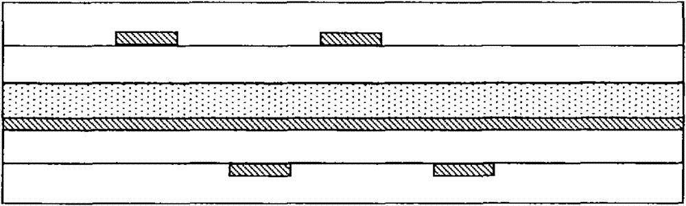
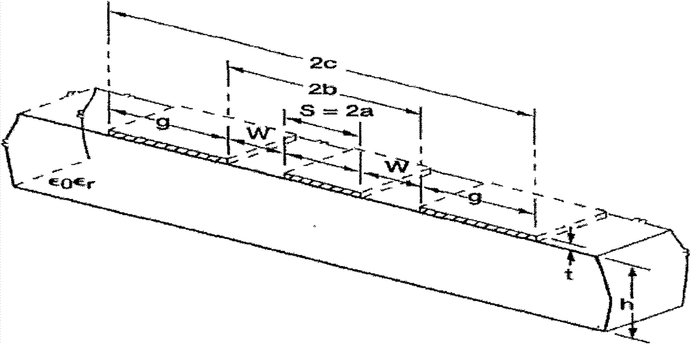
[0048] In order to facilitate the understanding of the present invention, the relevant knowledge of the CPW coplanar waveguide is firstly introduced. The coplanar waveguide is composed of three wires, the middle conductor is the signal line, and the wires on both sides are the ground plane, such as image 3 As shown, the signal is a time-varying signal when propagating, so the signal line and the ground plane are changing at any time. Its electrical characteristics such as characteristic impedance are determined by the width of the sign...


PUM


Abstract

The embodiment of the invention provides a printed circuit board, which comprises a hard board part and a soft board part, wherein the hard board part is in a micro-strip line design, and the reference ground of signals is a horizontal plane formed by an upper-layer conductor or a lower-layer conductor on the micro-strip line; and the soft board part is in a CPW (coplanar waveguide) design, and ground signals in the CPW structure of the soft board part are connected with ground signals of the hard board part. The embodiment of the invention also provides a design method of the printed circuit board. The scheme provided by the invention solves the problem that under the same PCB (printed circuit board) area, micro coaxial cables can not transmit a large number of G bit differential signals. In addition, the scheme provided by the invention also solves the problem of PCB layering brought by the fact that more than two flexible material core plates are needed for lamination in order to reduce the transmission difference loss of the G bit signals in the soft and hard combined PCB in the micro-strip line design method.

Description

technical field [0001] The invention relates to the field of electronic circuits, in particular, the invention relates to a printed circuit board and a design method thereof. Background technique [0002] With the rapid development of modern electrical technology, the data transmission rate between PCB (Printed Circuit Board, printed circuit board) boards is getting higher and higher. At present, a pair of differential lines can reach the transmission rate of 10G bits per second. More and more signal lines to increase the throughput rate of transmitted data. [0003] Design solutions for existing PCB boards have the following forms: [0004] 1) Use ordinary micro-coaxial cables; [0005] 2) Rigid-flex PCB designed with microstrip line design method. [0006] The solution using ordinary micro-coaxial cables has the following characteristics: [0007] The advantage is that the transmission rate of the single line is high; [0008] The disadvantage is that the number of si...

Claims


Application Information

Patent Timeline
Patent Type & Authority Patents(China)
IPC IPC(8): H05K1/14
Inventor 李军钟显成郭东王宏伟
Owner DATANG MOBILE COMM EQUIP CO LTD
Features
  • R&D
  • Intellectual Property
  • Life Sciences
  • Materials
  • Tech Scout
  • Unparalleled Data Quality
  • Higher Quality Content
  • 60% Fewer Hallucinations
Learn More