Consumable chip, consumable container and data writing method for consumable chip

A consumable chip, data writing technology, applied in the direction of instruments, electrical recording process applying charge pattern, equipment applying electrical recording process of charge pattern, etc. And other issues

Inactive Publication Date: 2012-03-21
ZHUHAI TIANWEI TECH DEV CO LTD
View PDF10 Cites 12 Cited by
  • Summary
  • Abstract
  • Description
  • Claims
  • Application Information

AI Technical Summary

Problems solved by technology

Moreover, the other side of the substrate is provided with an electronic module electrically connected to the electrical contact 34, and an interface unit, a control unit and a non-volatile memory are also provided on the electronic module. For the same reason, the chip 33 also has a The problem of slow writing data in volatile memory and affecting the work of laser printers
[0013] In addition, toner cartr

Method used


Image

  • Consumable chip, consumable container and data writing method for consumable chip
  • Consumable chip, consumable container and data writing method for consumable chip
  • Consumable chip, consumable container and data writing method for consumable chip

Examples


Embodiment Construction

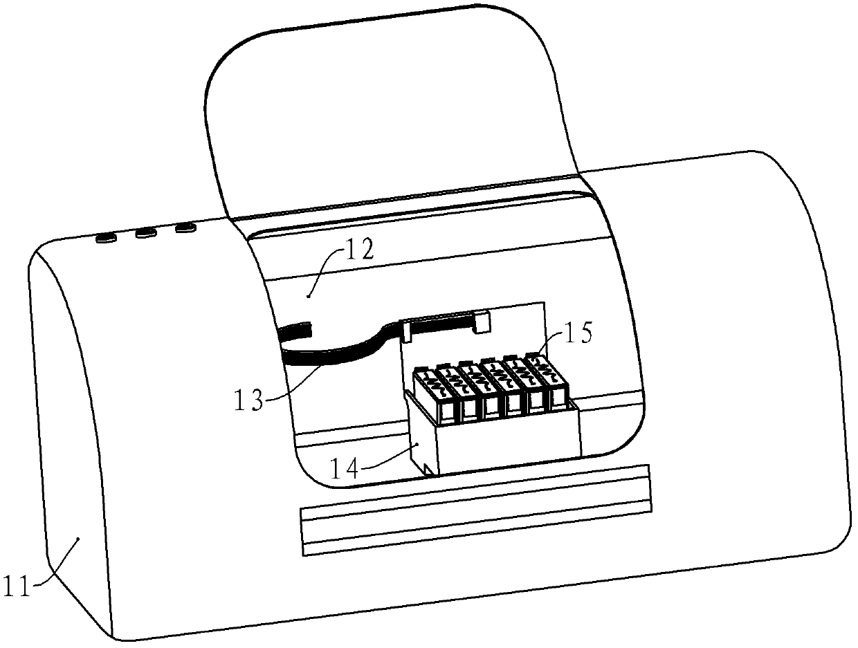
[0037] The consumables container of the present invention can be an ink cartridge installed on an inkjet printer, or a toner cartridge or a toner cartridge installed on a laser printer, copier, fax machine, or all-in-one machine. The present invention will be described in detail below in conjunction with various embodiments. illustrate.

[0038] Embodiment of consumable chip and its data writing method:

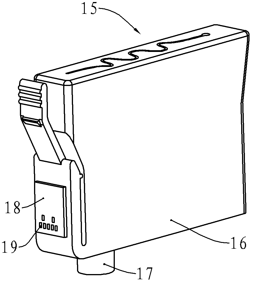
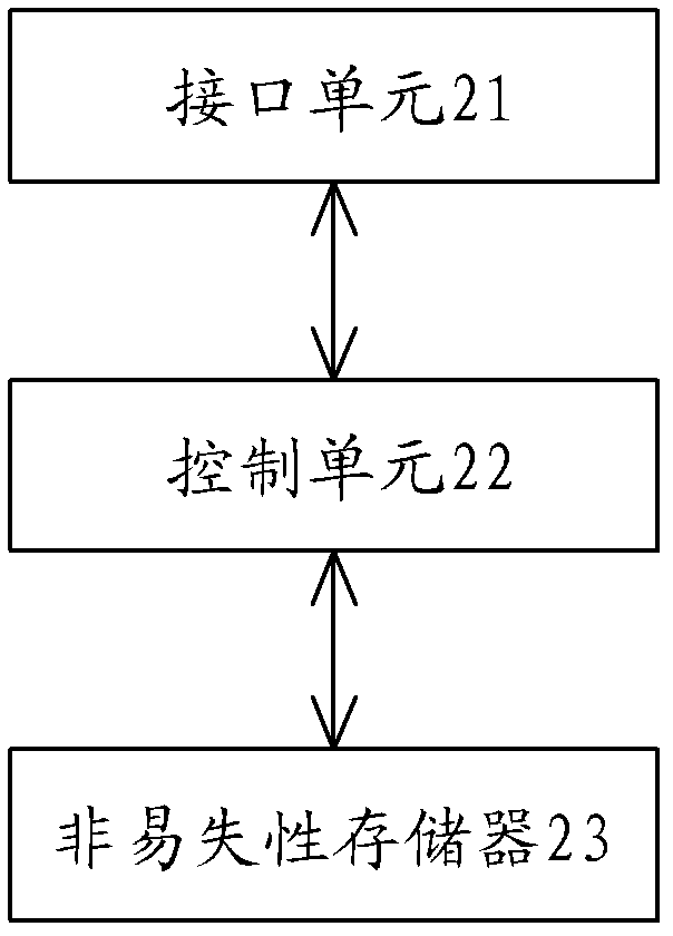
[0039] The consumable chip in this embodiment has a substrate, and one side of the substrate is provided with a plurality of electrical contacts as a communication unit for connecting with the electrical contacts of the inkjet printer. Of course, if the inkjet printer and the consumable chip communicate wirelessly, the communication unit is an antenna for wireless communication. On the other side of the substrate, there is an electronic module connected to the electrical contacts. The electrical principle block diagram of the electronic module is as follows: Figure 5 shown...


PUM


Abstract

The invention provides a consumable chip, a consumable container and a data writing method for the consumable chip. The chip is provided with a substrate, wherein the substrate is provided with a communication unit and an electronic module which is electrically connected with the communication unit; the electronic module is provided with an interface unit, a control unit for receiving a signal transmitted by the interface unit, and a nonvolatile memory connected with the control unit; and the control unit is provided with a data register for temporarily storing data which are not written into the nonvolatile memory in time. The method comprises the following steps that: the control unit receives data needing to be written into the nonvolatile memory, and judges whether the data size of the received data is greater than a preset data size, and if so, stores data exceeding the preset data size in the data register; and the control unit writes data within the preset data size into the nonvolatile memory, and writes the data in the data register into the nonvolatile memory. According to the invention, data transmitted by an imaging device can be completely written into the nonvolatile memory, and the work of the imaging device is not influenced.

Description

technical field [0001] The invention relates to the field of printing, in particular to a consumable chip mounted on a printing consumable, a consumable container equipped with the consumable chip, and a data writing method for the consumable chip. Background technique [0002] As a common office equipment, printers provide great convenience for modern office. Existing printers are divided into inkjet printers and laser printers. Inkjet printers use ink cartridges containing ink as consumable containers to spray ink on paper to form text or patterns that need to be printed on paper; laser printers use ink cartridges containing toner The toner cartridge is used as a consumable container to form text or patterns that need to be printed on the medium. [0003] see figure 1 , an existing color inkjet printer has a casing 11, figure 1 The inkjet printer is shown with the chassis 11 omitted. The machine core 12 of ink-jet printer is provided with in the casing 11, and is provi...

Claims


Application Information

Patent Timeline
IPC IPC(8): B41J2/175G03G15/08
Inventor 许兰秦正南
Owner ZHUHAI TIANWEI TECH DEV CO LTD
Why Eureka
Try Eureka