LED (light-emitting diode) luminous module and manufacturing method thereof

A light-emitting module and manufacturing method technology, applied in electrical components, electrical solid-state devices, circuits, etc., can solve the problems of dispersion, uneven refraction at the edge of the light spot, easy aging and deterioration of phosphors and packaging materials, and achieve uniform and good light color. Bukkake uniformity, simple connection circuit effect

Inactive Publication Date: 2012-03-28
郑伟
View PDF0 Cites 0 Cited by
  • Summary
  • Abstract
  • Description
  • Claims
  • Application Information

AI Technical Summary

Problems solved by technology

At present, there are two mainstream modular packaging schemes: one, after fixing dozens or hundreds of blue-light-emitting LED chips on the heat dissipation substrate, apply a uniform layer of yellow phosphor on the surface of the chip, and then use silica gel Or epoxy resin sealing; the disadvantage of this solution is that it cannot efficiently dissipate heat for the chip, making the phosphor and packaging materials easy to age and deteriorate. Therefore, high-power LED modules packaged with this solution rarely exceed 100W.
The second option is to use three-color LED chip packaging to realize high-power LED modules. Most of the methods are simply to arrange the chips of the same color into a straight array, and then arrange the arrays of different colors crosswise; the advantage of this method is that the chips The connection circuit is simple, but its biggest disadvantage is that under white light illumination, the edge of the spot is uneven, and it will cause dispersion when there is an object blocking it.

Method used


Image

  • LED (light-emitting diode) luminous module and manufacturing method thereof
  • LED (light-emitting diode) luminous module and manufacturing method thereof
  • LED (light-emitting diode) luminous module and manufacturing method thereof

Examples


Embodiment 1

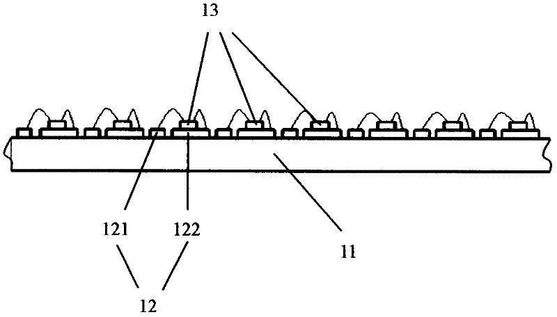
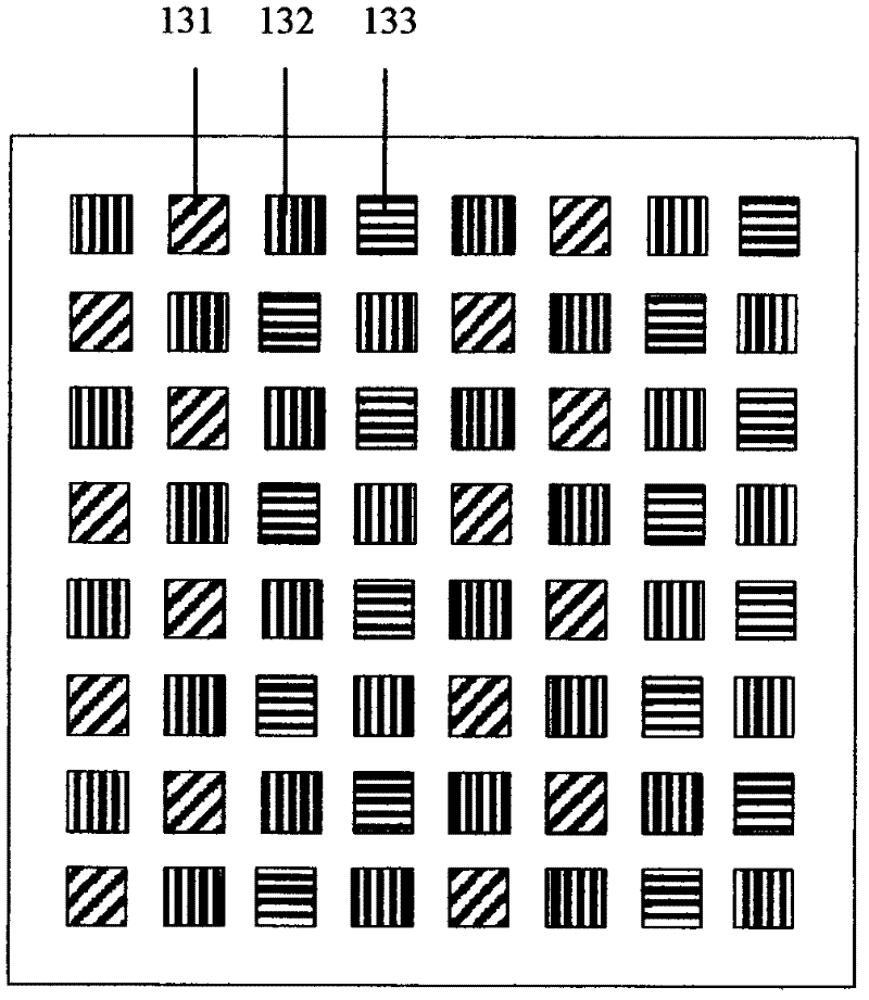
[0025] A kind of LED lighting module, its cross-sectional schematic diagram refers to figure 1 , which is characterized in that it includes an aluminum nitride ceramic substrate 11, an electrode 12 is arranged on the aluminum nitride ceramic substrate, and the electrode 12 is divided into a positive electrode 121 and a negative electrode 122, and may also be a positive electrode 122 and a negative electrode 121. The electrode 12 is provided with a three-primary-color LED chip array 13 , the three-primary-color LED chip array includes a red LED chip 131 , a green LED chip 132 , and a blue LED chip 133 , and the three-primary-color LED chip array is arranged in a Bayer manner.

[0026] In this embodiment, the Bayer arrangement is as follows figure 2 Schematic, it can be described as: the three-primary-color LED chips are arranged in the order of "...red, green, blue, green, red, green, blue-green..." in the odd-numbered rows, and the three-primary-color LED chips in the even-nu...

Embodiment 2

[0033] The present invention also provides a method for manufacturing an LED lighting module, comprising the following steps:

[0034] An aluminum nitride ceramic substrate is provided, and an electrode array is fabricated on the aluminum nitride ceramic substrate;

[0035] Provide a three-primary-color LED chip array, and arrange the three-primary-color LED chip array on the aluminum nitride ceramic substrate with electrodes fabricated in a Bayer manner;

[0036] Using the electrode array to connect chips of the same color in the three-primary-color LED chip array in series and / or in parallel.

[0037] In this embodiment, the Bayer arrangement can be described as: LED chips of three primary colors are arranged in the order of "...red, green, blue, green, red, green, blue, green..." in odd rows, and in even rows The three-primary-color LED chips are arranged in the order of "...green, blue, green, red, green, blue, green, red..."; of course, the order of the odd-numbered rows...


PUM


Abstract

The invention discloses a manufacturing method of an LED (light-emitting diode) luminous module. The invention also provides an LED luminous module manufactured based on the method. In the LED luminous module provided by the invention, an aluminum nitride ceramic base plate is used as a carrier; an electrode array and a tricolor LED chip array are arranged on the carrier; the tricolor LED chip array is ranked in a Bayer mode; and through the electrode array, chips with the same color in the tricolor LED chip array are connected in series and/or in parallel.

Description

technical field [0001] The invention relates to the field of high-power LED lighting, in particular to an LED light-emitting module and a manufacturing method of the LED light-emitting module. technical background [0002] As a lighting source, high-power LEDs have the advantages of small size, less power consumption, less heat generation, fast response, low safety voltage, good weather resistance, and good directionality. Therefore, high-power LEDs are ideal light sources for indoor and outdoor lighting. At present, the development trend of high-power LED is modularization, that is, dozens or hundreds of LED chips are packaged on a single small-area substrate to form a high-power LED light-emitting module. At present, there are two mainstream modular packaging schemes: one, after fixing dozens or hundreds of blue-light-emitting LED chips on the heat dissipation substrate, apply a uniform layer of yellow phosphor on the surface of the chip, and then use silica gel Or epoxy ...

Claims


Application Information

Patent Timeline
Patent Type & Authority Applications(China)
IPC IPC(8): H01L25/075H01L33/64H01L33/38H01L33/00
Inventor 郑伟李萌萌
Owner 郑伟
Why Eureka
Try Eureka