Substrate of liquid crystal display device, liquid crystal display device and manufacturing method for liquid crystal display device

A technology of a liquid crystal display device and a manufacturing method, which is applied in the directions of optics, instruments, nonlinear optics, etc., and can solve problems such as timely transmission of signals, poor bonding of the frame glue 60, and influence on the display range of the liquid crystal display device, so as to expand the range and improve range effect

Inactive Publication Date: 2012-04-04
SHENZHEN CHINA STAR OPTOELECTRONICS TECH CO LTD
View PDF5 Cites 55 Cited by
  • Summary
  • Abstract
  • Description
  • Claims
  • Application Information

AI Technical Summary

Problems solved by technology

[0005] In addition, due to the uneven diffusion of the alignment liquid at the coating boundary, it is necessary to reserve an end distance X from the boundary of the visible area 101 and to keep a certain distance from the area where the sealant 60 is installed so that the alignment liquid will not spread. In the installation area of ​​the frame glue 60, the frame glue 60 is poorly bonded and the gold ball 70 cannot transmit the signal on the array substrate to the color filter substrate in time. Due to these factors, the coating boundary of the alignment liquid is greatly affected , which in turn affects the display range of the liquid crystal display device

Method used


Image

  • Substrate of liquid crystal display device, liquid crystal display device and manufacturing method for liquid crystal display device
  • Substrate of liquid crystal display device, liquid crystal display device and manufacturing method for liquid crystal display device
  • Substrate of liquid crystal display device, liquid crystal display device and manufacturing method for liquid crystal display device

Examples


Embodiment Construction

[0033] The present invention will be further described below in conjunction with the accompanying drawings and preferred embodiments.

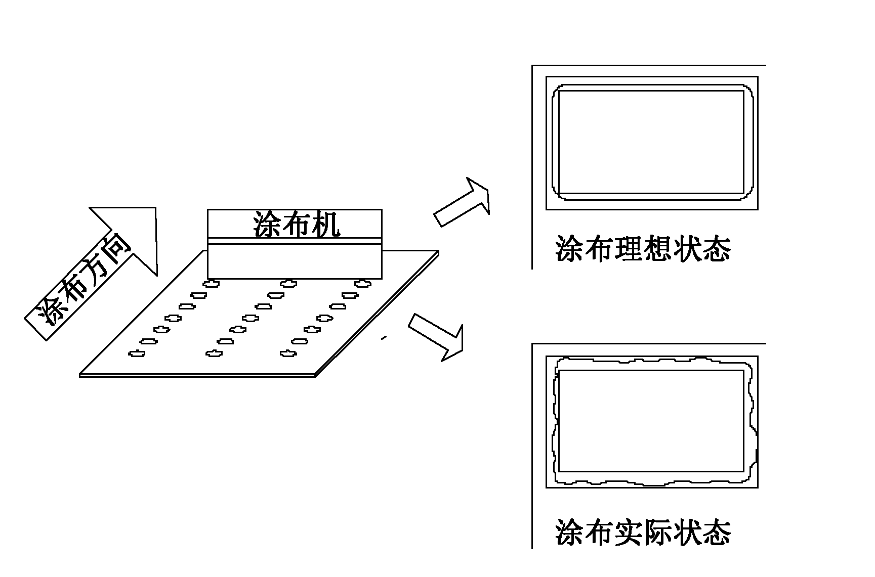
[0034] The present invention provides a liquid crystal display device and a manufacturing method thereof. The liquid crystal display device includes a substrate, and on the substrate, a boss or a groove for preventing the diffusion of the alignment liquid is provided on the boundary of the area where the alignment liquid needs to be coated; The substrate includes an array substrate and a color filter substrate of a liquid crystal display device.

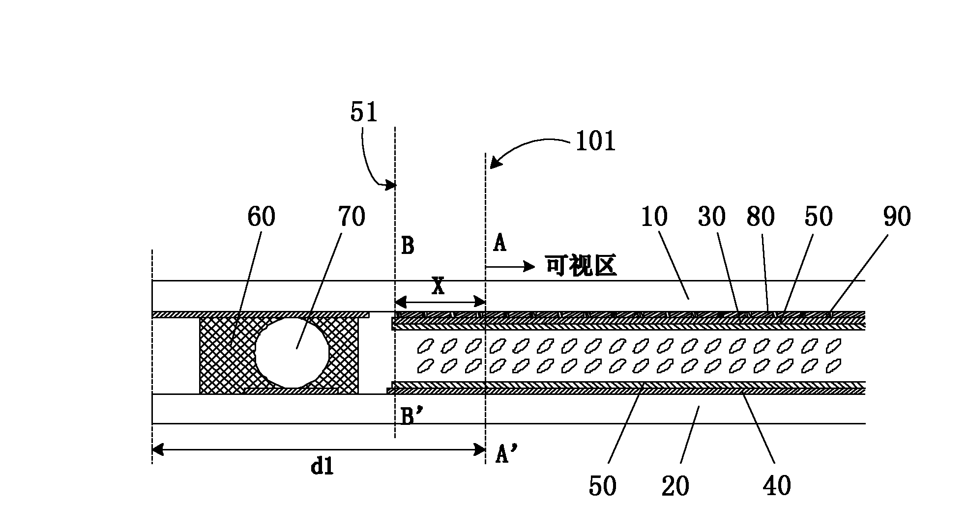
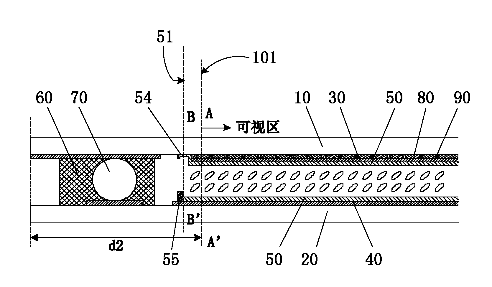
[0035] Such as image 3 Shown is an embodiment of the present invention, and shown in the figure is a structural cross-sectional view of a liquid crystal panel of a liquid crystal display device, which includes an array substrate and a color filter substrate facing each other; the color filter substrate includes an upper glass 10, and the upper glass 10 is arranged There is a color film 80, a black ...


PUM


Abstract

The invention discloses a substrate of a liquid crystal display device, the liquid crystal display device and a manufacturing method for the liquid crystal display device. A lug boss or a groove used for preventing alignment liquid from diffusing is formed on the boundary of an area in which the alignment liquid is required to be coated on the substrate. Because the lug boss or the groove used for preventing the alignment liquid from diffusing is formed on the substrate of the liquid crystal display device, the lug boss can prevent the alignment liquid from diffusing and the groove can absorb the diffusing alignment liquid, the alignment liquid is prevented from diffusing on the substrate with surface segment difference and forming an uneven boundary, and a uniform boundary is formed, so that the boundary of a visible area of the liquid crystal display device further deviates to the boundary of an alignment layer, and the range of the visible area is widened. In addition, because of the prevention of the lug boss or the groove, the lug boss or the groove can deviate to the frame glue, namely the boundary of the alignment layer can deviate to frame glue, and the range of the visible area is further widened.

Description

technical field [0001] The invention relates to the field of liquid crystal display, and more specifically, to a substrate of a liquid crystal display device, a liquid crystal display device and a manufacturing method thereof. Background technique [0002] The liquid crystal display panel is the main component of the liquid crystal display device, which includes an upper array substrate, a color filter substrate, and a liquid crystal arranged between the array substrate and the color filter substrate, wherein the liquid crystal is aligned through an alignment layer coated on the substrate, so that Liquid crystals are aligned in a specific direction. [0003] Such as figure 1 Shown is the alignment layer coating process of the glass substrate of the existing liquid crystal panel. Since the alignment liquid (PI) will diffuse through surface tension, and the surface state of the edge of the glass substrate is not uniform and flat, the diffusion of the alignment liquid will be ...

Claims


Application Information

Patent Timeline
Patent Type & Authority Applications(China)
IPC IPC(8): G02F1/1337G02F1/1335G02F1/1339G02F1/1333
CPCG02F1/1337G02F1/1333G02F1/133711G02F1/133388
Inventor 吴鸿杰施翔尹詹政川廖炳杰
Owner SHENZHEN CHINA STAR OPTOELECTRONICS TECH CO LTD
Why Eureka
Try Eureka