
Liquid crystal display device and method for manufacturing transparent electrode

A technology of liquid crystal display devices and transparent electrodes, which is applied in nonlinear optics, instruments, optics, etc., can solve the problems of high off-state transmittance, disordered orientation of liquid crystal molecules 8a, and decreased contrast, so as to suppress light leakage and disorder , to improve the effect of contrast

Inactive Publication Date: 2014-08-13
HOSIDEN CORP
View PDF4 Cites 0 Cited by
  • Summary
  • Abstract
  • Description
  • Claims
  • Application Information

AI Technical Summary

Problems solved by technology

[0013] In such trapezoidal first and second strip-shaped transparent electrodes 3a and 3b, as Image 6 Shown by the arrows of the solid lines in (b), the electric field generated by the off-state voltage applied to these first and second strip-shaped transparent electrodes 3a and 3b, the first and second strip-shaped transparent electrodes in the pixel The central parts of the electrodes 3a and 3b (pixel central parts) are neatly substantially parallel to the direction perpendicular to the first and second transparent substrates 5a and 5b, but the first and second strip-shaped transparent electrodes 3a and 3b in the pixel The end portion (the peripheral portion of the pixel) is not substantially parallel to the direction perpendicular to the first and second transparent substrates 5a and 5b, but becomes an oblique electric field, and the oblique electric field makes the alignment of the liquid crystal molecules 8a in the non-selected pixels creates a disorder, so if Image 6 As indicated by the hollow arrows in (b), light leaks around the non-selected pixels, which increases the off-state transmittance and lowers the contrast.

Method used


Image

  • Liquid crystal display device and method for manufacturing transparent electrode
  • Liquid crystal display device and method for manufacturing transparent electrode
  • Liquid crystal display device and method for manufacturing transparent electrode

Examples


Embodiment Construction

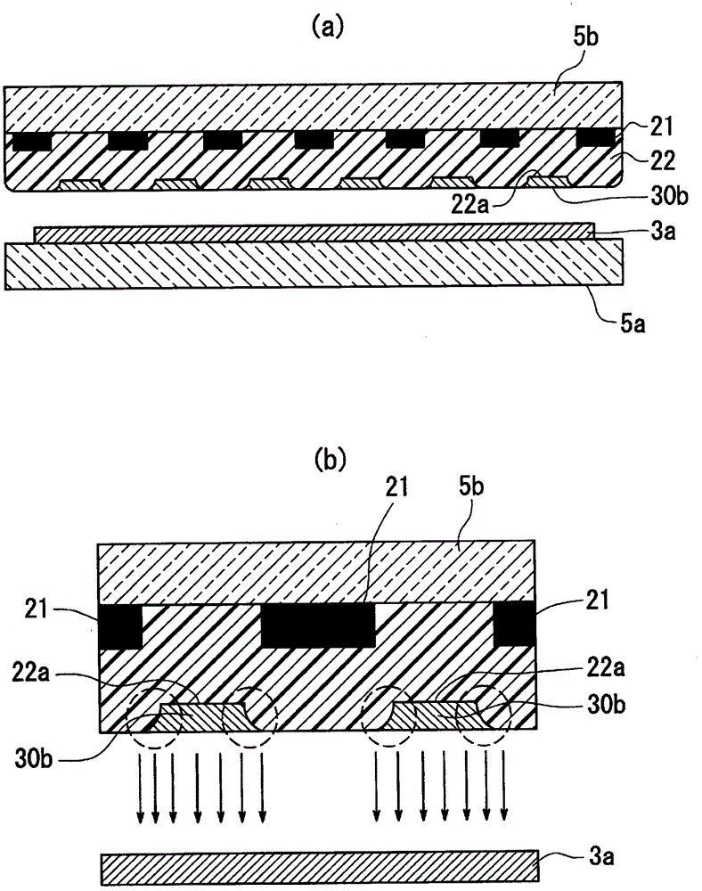
[0038] Below, refer to figure 1 Embodiments of the present invention will be described. figure 1 It is a schematic cross-sectional view showing a liquid crystal display device having a simple matrix electrode structure of the present invention, (a) is a schematic cross-section showing the shape of the first and second strip-shaped transparent electrodes, and (b) is a schematic cross-sectional view showing the shape of the first and second strip-shaped transparent electrodes. A schematic cross-sectional view of an electric field generated by an off-state voltage applied between the first and second transparent electrodes. In addition, in figure 1 The display device shown in is characterized by the structure of the second transparent electrode and its manufacturing method, and other structures and Figure 4 The vertical alignment type liquid crystal display devices shown in are the same, and therefore the same reference numerals are attached to the same structural parts, an...


PUM


Abstract

The present invention provides a liquid crystal display device capable of suppressing light leakage from peripheral portions of non-selected pixels and improving contrast without reducing the aperture ratio of pixels. The liquid crystal display device 1 includes the following structures: first and second transparent substrates 5a and 5b, facing each other and having a predetermined interval; a liquid crystal layer 8, disposed between the respective opposing faces of the first and second transparent substrates 5a and 5b ; The first strip-shaped transparent electrode 3a, which is formed on the surface of the first transparent substrate 5a opposite to the second transparent substrate 5b and is in a stripe shape; the transparent resin film 22, which is on the second transparent substrate 5b and the second transparent substrate 5b. On the surface opposite to a transparent substrate 5a, a transparent resin film is formed after forming a stripe-shaped black film 21 along the direction perpendicular to the first strip-shaped transparent electrode 3a, and at a position between the black film 21 The corresponding film surface has an inverted trapezoidal concave portion 22a; the second strip-shaped transparent electrode 30b, which is in an inverted trapezoidal shape, is formed in the concave portion 22a of the resin film 22 .

Description

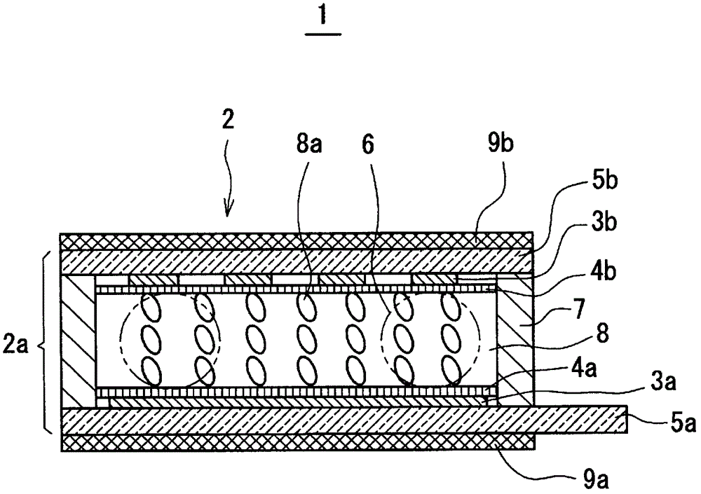
technical field [0001] The present invention relates to a liquid crystal display device having a simple matrix electrode structure and a method for manufacturing a transparent electrode. Background technique [0002] figure 2 It is a sectional view showing a vertical alignment type liquid crystal display device which is an example of a liquid crystal display device having a simple matrix electrode structure. The vertical alignment type liquid crystal display device 1 includes a liquid crystal panel 2 and displays an image using the liquid crystal panel 2 . [0003] In the liquid crystal panel 2, a first strip-shaped transparent electrode 3a made of ITO (indium tin oxide) or the like is formed on one side of a first transparent substrate 5a made of a glass plate or the like. A first alignment film 4a is formed on the strip-shaped transparent electrode 3a, and an alignment rubbing process is applied to the first alignment film 4a. A second strip-shaped transparent electrode...

Claims


Application Information

Patent Timeline
Patent Type & Authority Patents(China)
IPC IPC(8): G02F1/1343G02F1/1335
CPCG02F1/133512G02F1/134336G02F1/13439G02F1/1335G02F1/1343
Inventor 石川拓幸守屋光雄泷川满
Owner HOSIDEN CORP
Learn More