Supercharge Your Innovation With Domain-Expert AI Agents!

Isolation structure and manufacturing method thereof as well as semiconductor device with isolation structure

An isolation structure, semiconductor technology, applied in the direction of semiconductor/solid-state device manufacturing, electrical components, circuits, etc., can solve the problems of the effectiveness of the gate dielectric layer and the inability to effectively reduce the threshold voltage of transistors, and achieve the effect of reducing the impact.

Inactive Publication Date: 2012-04-18
INST OF MICROELECTRONICS CHINESE ACAD OF SCI +1
View PDF6 Cites 0 Cited by
  • Summary
  • Abstract
  • Description
  • Claims
  • Application Information

AI Technical Summary

Problems solved by technology

[0006] The purpose of the present invention is to solve at least one of the above-mentioned problems in the prior art, especially to solve the problem that the effectiveness of the gate dielectric layer is affected by the narrow channel effect, which leads to the problem that the threshold voltage of the transistor cannot be effectively reduced

Method used


Image

  • Isolation structure and manufacturing method thereof as well as semiconductor device with isolation structure
  • Isolation structure and manufacturing method thereof as well as semiconductor device with isolation structure
  • Isolation structure and manufacturing method thereof as well as semiconductor device with isolation structure

Examples


Embodiment Construction

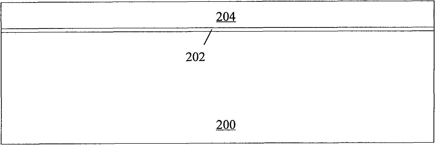
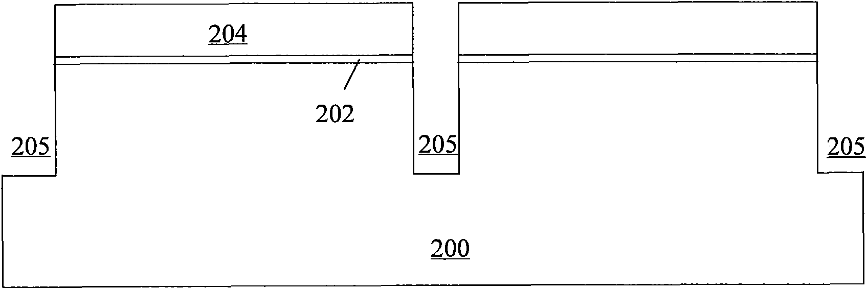
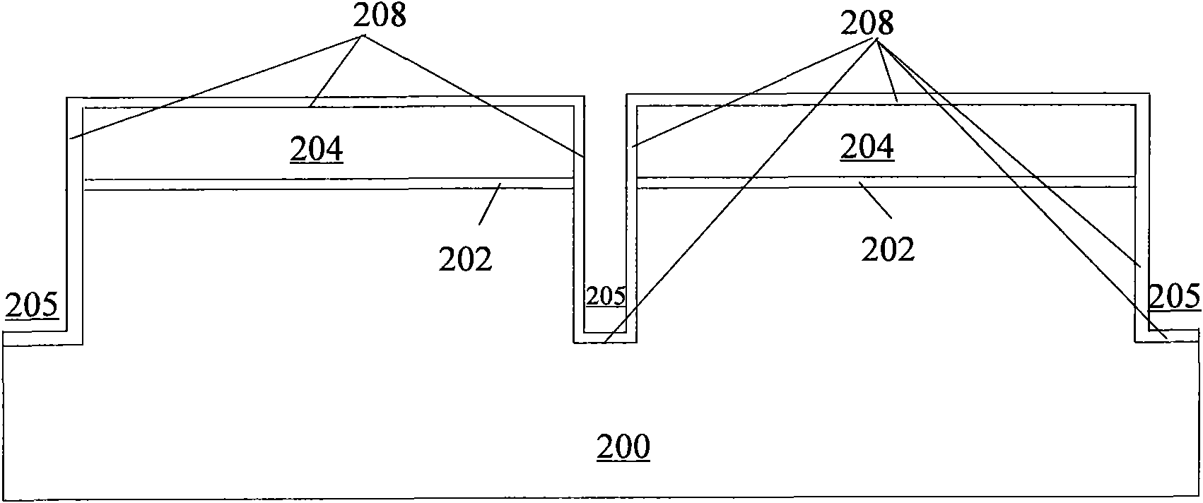
[0014] The following disclosure provides many different embodiments or examples for implementing different structures of the present invention. To simplify the disclosure of the present invention, components and arrangements of specific examples are described below. Of course, they are only examples and are not intended to limit the invention. Furthermore, the present invention may repeat reference numerals and / or letters in different instances. This repetition is for the purpose of simplicity and clarity and does not in itself indicate a relationship between the various embodiments and / or arrangements discussed. In addition, various specific process and material examples are provided herein, but one of ordinary skill in the art will recognize the applicability of other processes and / or the use of other materials. Additionally, configurations described below in which a first feature is "on" a second feature may include embodiments where the first and second features are form...


PUM

PropertyMeasurementUnit
Thicknessaaaaaaaaaa

Abstract

The invention discloses an isolation structure of a semiconductor device, a manufacturing method of the isolation structure and the semiconductor device with the isolation structure, relating to the field of semiconductor manufacture. The isolation structure comprises a groove, a lanthanum-rich oxide layer and an isolation material, wherein the groove is embedded into the semiconductor substrate; the lanthanum-rich oxide layer covers the bottom wall and the side wall of the groove; and the isolation material is positioned in the groove on the lanthanum-rich oxide layer. According to the invention, the lanthanum-rich oxide layer is formed in the isolation structure; a lanthanum element is diffused to a gate dielectric layer, so that the influence caused by the narrow channel effect can be reduced and the threshold voltage of the device can be adjusted. The embodiment of the invention is suitable for a high-k / metal gate process in the semiconductor device process.

Description

technical field [0001] The present invention relates to an isolation structure of a semiconductor device and a manufacturing method thereof, in particular to an isolation structure and a manufacturing method thereof which use a lanthanum-rich oxide layer to reduce the influence caused by the narrow channel effect and simultaneously adjust the threshold voltage . Background technique [0002] As semiconductor technology advances, the size of transistors continues to shrink, increasing the speed of devices and systems. In this size-reduced transistor, the gate dielectric layer such as SiO 2 The thickness also becomes thinner. However, when SiO 2 When the thickness is thin to a certain extent, it will no longer be able to play the role of insulation well, and it is easy to generate leakage current from the gate to the active region. This greatly deteriorates device performance. [0003] For this purpose, instead of conventional SiO 2 / polysilicon gate stack, and proposed ...

Claims


Application Information

Patent Timeline
IPC IPC(8): H01L21/762
Inventor 骆志炯钟汇才尹海洲朱慧珑
Owner INST OF MICROELECTRONICS CHINESE ACAD OF SCI
Features
  • R&D
  • Intellectual Property
  • Life Sciences
  • Materials
  • Tech Scout
  • Unparalleled Data Quality
  • Higher Quality Content
  • 60% Fewer Hallucinations
Learn More