A kind of gan-based enhanced hemt device and its preparation method

An enhanced device technology, applied in semiconductor/solid-state device manufacturing, semiconductor devices, electrical components, etc., can solve problems such as low threshold voltage, reduced gate control capability, and current collapse, so as to reduce design difficulty and cost, Achieving enhanced device effects

Inactive Publication Date: 2017-07-14
INST OF SEMICONDUCTORS - CHINESE ACAD OF SCI
View PDF5 Cites 0 Cited by
  • Summary
  • Abstract
  • Description
  • Claims
  • Application Information

AI Technical Summary

Problems solved by technology

[0005] 1. Due to the polarization characteristics of the material itself, there is a high concentration of two-dimensional electron gas at the heterojunction interface, so that the device is in a conduction state under zero gate bias, that is, a depletion device (normally open), and its The circuit design is much more complicated than the enhanced (normally closed), which increases the difficulty and cost of circuit design
[0006] 2. From the perspective of safety, especially for devices used in the high-voltage field, the device is required to be in an off state, and the depletion device brings a great potential safety hazard
[0007] 3. From the perspective of energy saving, due to the zero gate voltage, the state-depleted device is in the conduction state, which will cause unnecessary energy loss
However, the concave gate etching process is difficult to control accurately, and it is easy to cause damage, which will cause current collapse and deteriorate the reliability of the device. At the same time, the threshold voltage is not high; F-based ion implantation will also bring a series of stability problems.
Whether it is concave gate etching or F-based ion implantation will cause damage to the material, although a certain amount of damage can be eliminated after annealing, the residual damage will still adversely affect the stability and reliability of the device, and the repeatability of the process It is not high; growing single-layer p-GaN or single-layer p-AlGaN on the gate is a relatively reliable method for realizing enhancement devices, but due to factors such as self-compensation effects and high activation energy of acceptor impurities, making The incorporation efficiency of acceptor doping atoms is low, and it is difficult to realize p-type GaN and AlGaN materials with high doping concentration, so the thickness of p-GaN or p-AlGaN needs to be relatively thick, but thick p-GaN or p- AlGaN will reduce the gate control ability and cause device performance degradation

Method used


Image

  • A kind of gan-based enhanced hemt device and its preparation method
  • A kind of gan-based enhanced hemt device and its preparation method
  • A kind of gan-based enhanced hemt device and its preparation method

Examples


Embodiment Construction

[0037] In order to make the object, technical solution and advantages of the present invention clearer, the present invention will be described in further detail below in conjunction with specific embodiments and with reference to the accompanying drawings.

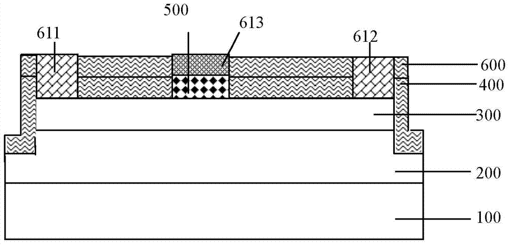
[0038] figure 1 It is a schematic structural diagram of a GaN-based enhancement mode HEMT device according to an embodiment of the present invention, such as figure 1 As shown, in an embodiment of the present invention, the GaN-based enhanced HEMT device includes: a substrate 100, a GaN intrinsic layer 200, a barrier layer 300, a high hole concentration structure layer 500, a first metal electrode 611, a second The second metal electrode 612, the third metal electrode 613, the passivation medium layer 400 and the passivation protection layer 600, wherein:

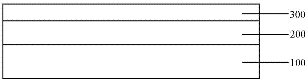
[0039] The GaN intrinsic layer 200 and the barrier layer 300 are sequentially grown on the substrate 100;

[0040] The high hole concentration structure layer 500 co...


PUM

PropertyMeasurementUnit
thicknessaaaaaaaaaa
thicknessaaaaaaaaaa
thicknessaaaaaaaaaa

Abstract

The invention discloses a novel GaN-based enhanced HEMT device. The novel GaN-based enhanced HEMT device comprises a GaN intrinsic layer, a barrier layer, a high-hole-concentration structural layer, a first metal electrode, a second meta electrode, a third metal electrode, a passivating dielectric layer and a passivating protection layer, wherein the GaN intrinsic layer and the barrier layer sequentially grow on a substrate, the high-hole-concentration structural layer covers the partial area of the upper surface of the barrier layer, the first metal electrode and the second meta electrode are located in the partial area which is not covered by the high-hole-concentration structural layer, of the upper surface of the barrel layer, the third metal electrode covers the upper surface of the high-hole-concentration structural layer, the passivating dielectric layer covers the upper surface of the obtained substrate and forms a table top graph, and the passivating protection layer covers the upper surface of the passivating dielectric layer. The invention further discloses a manufacturing method of the novel GaN-based enhanced HEMT device. The novel GaN-based enhanced HEMT device is high in reliability and good in repeatability, adjustment of device threshold voltage can be achieved by selecting different component gradual change ranges, different nitride alloys and the dosage concentration and thickness of the different nitride alloys, and the manufactured device can meet different requirements.

Description

technical field [0001] The invention relates to the field of manufacturing semiconductor devices, in particular to a GaN-based enhanced HEMT device and a preparation method thereof, in which a novel p-type multi-element nitride alloy with gradual composition is added to a GaN heterojunction structure. Background technique [0002] GaN material has unique advantages in the preparation of high-voltage, high-temperature, high-power and high-density integrated electronic devices because of its large band gap, high critical breakdown electric field, and high thermal conductivity. [0003] GaN materials can form heterojunction structures with AlGaN, InAlN and other materials. Due to the spontaneous polarization and piezoelectric polarization effects of barrier layer materials such as AlGaN or InAlN, a high-concentration and high-mobility two-dimensional electron gas (2DEG) will be formed at the heterojunction interface. This characteristic can not only improve the carrier mobilit...

Claims


Application Information

Patent Timeline
Patent Type & Authority Patents(China)
IPC IPC(8): H01L29/778H01L21/335
CPCH01L29/0684H01L29/66431H01L29/778
Inventor 贾利芳何志刘志强李迪樊中朝程哲梁亚楠王晓东杨富华
Owner INST OF SEMICONDUCTORS - CHINESE ACAD OF SCI
Why Eureka
Try Eureka