Probe card and test method

A test method and probe card technology, applied in the field of probe cards, can solve the problems of increasing the burden of the manufacturing process and the complicated test process, etc.

Active Publication Date: 2012-05-02
ADVANCED SEMICON ENG INC
View PDF5 Cites 9 Cited by
  • Summary
  • Abstract
  • Description
  • Claims
  • Application Information

AI Technical Summary

Problems solved by technology

In this way, the testing process is relatively complicated and relatively increases the burden on the manufacturing process

Method used


Image

  • Probe card and test method
  • Probe card and test method
  • Probe card and test method

Examples


Embodiment Construction

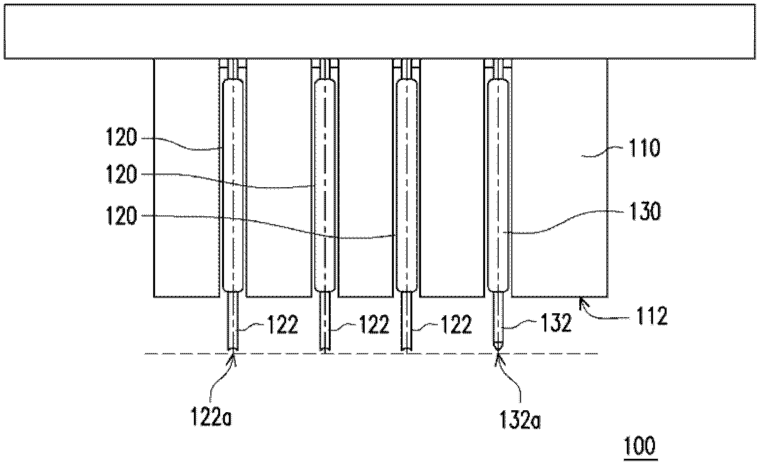
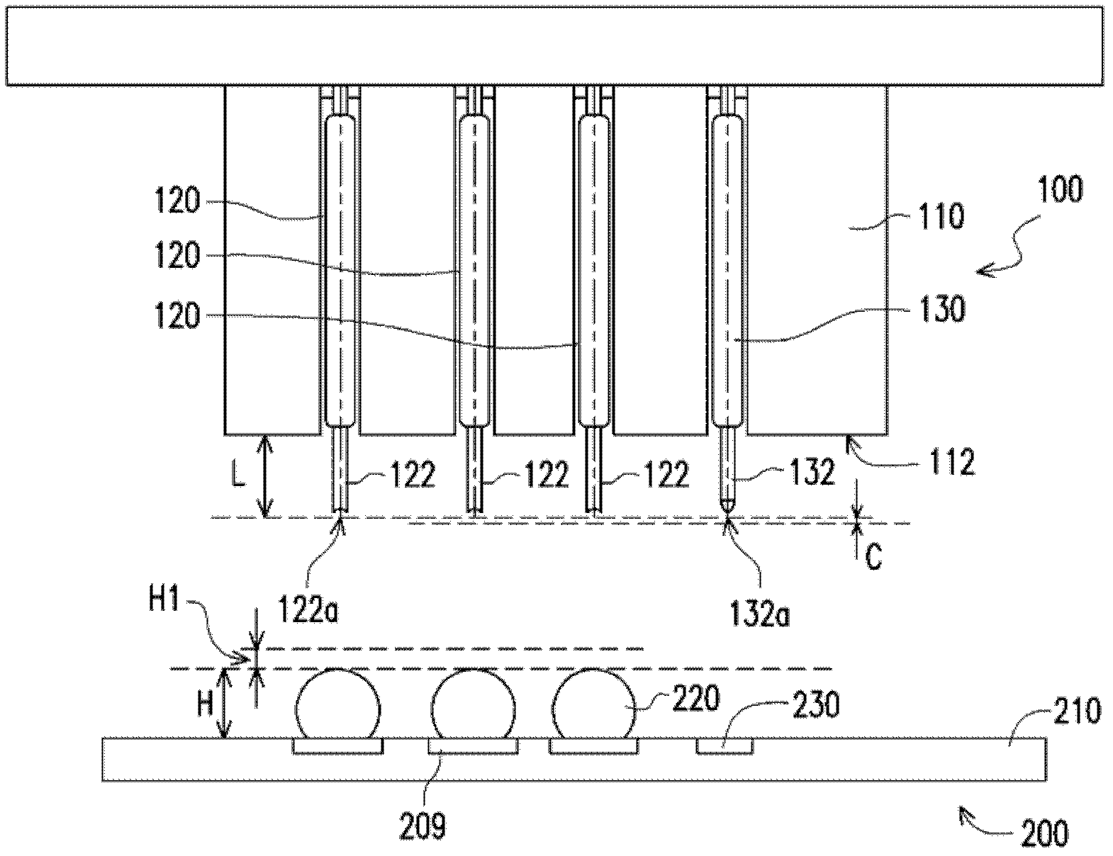
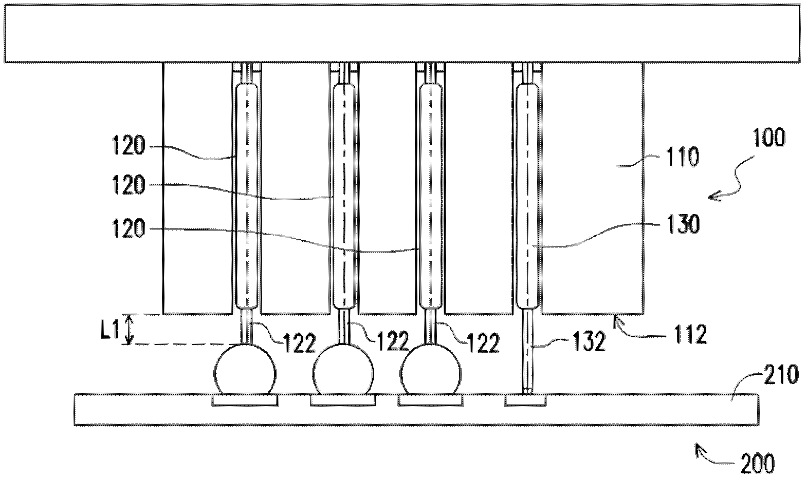
[0056] Please refer to figure 1 , which shows a probe card 100 according to an embodiment of the present invention. The probe card 100 includes a base body 110 , a plurality of first probes 120 and a plurality of second probes 130 . The base body 110 is mainly used to fix the first probe 120 and the second probe 130 , and then may be connected to a circuit board, an adapter board, etc. for testing common components (not shown in the figure). The first probe 120 and the second probe 130 are respectively inserted in the base body 110 and are substantially parallel to each other. Each first probe 120 and each second probe 130 respectively have a first telescopic end 122 and a second telescopic end 132 protruding from a surface 112 of the base body 110 , and each first telescopic end 122 has a first The end surface 122a is substantially flush with a second end surface 132a of each second telescopic end 132 . In this embodiment, each first telescopic end 122 has a first stroke t...


PUM


Abstract

The invention discloses a probe card and a test method. The probe card integrates multiple probes with different strokes. The multiple probes with the different strokes can contact connecting points at different heights when facing to the connecting points at the different heights on an object to be tested, so that the object to be tested can be tested. In addition, the test method employing the probe card is also disclosed.

Description

technical field [0001] The invention relates to a test device and a test method, and in particular to a probe card suitable for testing semiconductor components and a test method using the probe card. Background technique [0002] The electrical test of an integrated circuit chip (IC chip) is very important in each stage of a semiconductor process. Each IC chip must be tested in wafer and package form to ensure its electrical function. [0003] Wafer test (wafer test) is to make the test machine and probe card (probe card) form a test circuit, the probe (probe pin) on the probe card is directly connected to the pad (pad) or bump (bump) on the wafer ) contact, to use the probe to detect each chip on the wafer, thereby leading to the chip signal, and sending the chip signal data to the test machine for analysis and judgment. In this way, before the packaging step, chips with poor electrical properties and functions can be filtered out in advance, so as to avoid increasing th...

Claims


Application Information

Patent Timeline
IPC IPC(8): G01R1/073
Inventor 曹育诚
Owner ADVANCED SEMICON ENG INC
Why Eureka
Try Eureka