Photoelectric sensing detector based on seamless splicing and manufacturing method thereof

A seamless splicing, photoelectric sensing technology, applied in the field of radiation detection

Inactive Publication Date: 2012-05-09
SHANGHAI RES CENT OF BIOMEDICAL ENG
View PDF5 Cites 13 Cited by
  • Summary
  • Abstract
  • Description
  • Claims
  • Application Information

AI Technical Summary

Problems solved by technology

[0005] The purpose of the present invention is to provide a photoelectric sensing detector based on seamless splicing and can be formed into any angle and its preparation method, so as to overcome the dilemma faced by the existing large-area flat panel detectors in the field of non-planar radiation detection

Method used


Image

  • Photoelectric sensing detector based on seamless splicing and manufacturing method thereof
  • Photoelectric sensing detector based on seamless splicing and manufacturing method thereof
  • Photoelectric sensing detector based on seamless splicing and manufacturing method thereof

Examples


Embodiment 1

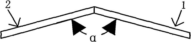
[0028] see figure 1 , which is a schematic cross-sectional view of two adjacent detector modules 1 and 2 in the photoelectric sensing detector based on seamless splicing of the present invention, the detector modules 1 and 2 are spliced ​​into an angle shape in a seamless splicing manner, that is, the detector module The angle between 1 and detector module 2 is α, where 0<α<360°, and both detector module 1 and detector module 2 are photosensitive array modules, which can be coupled to the scintillator layer, and the structures of the two same.

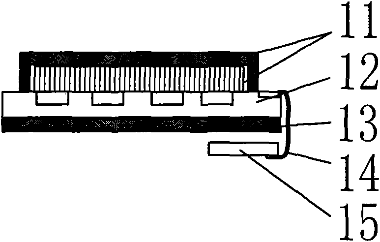
[0029] see you again figure 2 , which is a schematic diagram of the modular unit structure of the stitched detector. The detector module unit includes: a base plate 13 , a photosensitive element array 12 , a scintillator layer and an encapsulation layer 11 , a processing circuit 15 , and an interconnection circuit 14 and the like. It should be noted that if the array of photosensitive elements can directly detect radiation (ie X-ra...

Embodiment 2

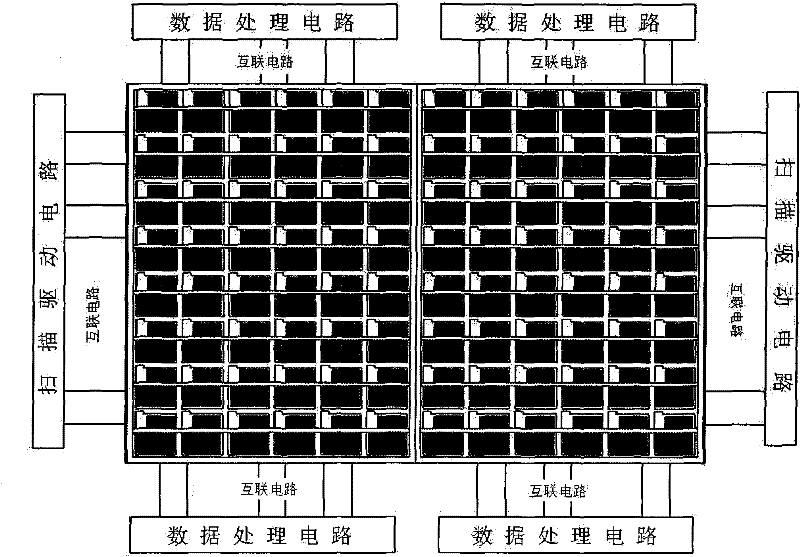
[0038] See Figure 5 , which is a schematic cross-sectional view of the detector modules 1', 2' and 3' in the photoelectric sensing detector based on seamless splicing of the present invention, and the detector modules 1', 2' and 3' are spliced ​​into a seamless splicing manner Angled, that is, the angle between detector modules 1' and 2 is α1, and the angle between detector modules 2' and 3' is α2, where 0 Image 6 As shown, in the same detector module, the interconnection circuit connected to the scanning drive circuit and the interconnection circuit connected to the data processing circuit are arranged on opposite sides of the photosensitive element array module, so that the remaining opposite sides can be used for seamless splicing, Further, a photoelectric sensor detector formed by seamless splicing of three or more photosensitive element array modules is formed.

Embodiment 3

[0040] See Figure 7a with Figure 7b , which is a schematic cross-sectional view of the detector modules 1"2", 3" and 4" in the photoelectric sensing detector based on seamless splicing of the present invention, between the detector modules 1" and 2", and the detector module 3" and 4" is α1; the angle between detector modules 1" and 3" and between detector modules 2" and 4" is α2, where 0 Figure 4 As shown, in the same photosensitive element array module, interconnection circuits are provided only on both sides, and the interconnection circuit connected to the scanning drive circuit and the interconnection circuit connected to the data processing circuit are arranged on adjacent two sides of the photosensitive element array module. A photoelectric sensing detector comprising four detector modules is formed.


PUM

PropertyMeasurementUnit
angleaaaaaaaaaa

Abstract

The invention provides a photoelectric sensing detector based on seamless splicing and a manufacturing method thereof. The photoelectric sensing detector is composed by seamlessly splicing at least two photoelectric sensing detector modules which form a certain angle, wherein each detector module can work independently. The detector module is structured as follows: a soleplate capable of baffling radiation rays is used as a base; light-sensing elements which form a light-sensing element array used for converting sensed photon signals into electric signals are fixed at the surface of one side of the soleplate; a treatment circuit used for scanning the light-sensing element array and capable of carrying out data treatment to the electric signals sent by each light-sensing element and finally transmitting the treated signals to a device which can form corresponding images is arranged at the surface of the other side of the soleplate; and meanwhile, circuits connected with each other are used for electrically connecting the light-sensing element array and the treatment circuit. A radiation detector manufactured through the method can effectively inhibit ray scattering and crosstalk among modules and can be well suitable for the radiation detection field of non-planar structures.

Description

technical field [0001] The invention relates to a photoelectric sensing detector based on seamless splicing and a preparation method thereof, belonging to the technical field of radiation detection. Background technique [0002] In industrial non-destructive testing and medical industry, radiation detector technology is widely used, and with the development of semiconductor technology, the dynamic range and quantum detection efficiency of flat panel detectors used for radiation detection have been greatly improved. Therefore, in Radiographic imaging systems for medical treatment and non-destructive testing are widely used. In the field of digital X-ray imaging (DR), large-size flat-panel detectors up to 17 inches square (43cm*43cm) have been widely used. [0003] However, in some special fields, it is often desired that the radiation-receiving detector be arc-shaped or that the photosensitive surface of the detector can have a certain angle to form a fan beam or a similar fa...

Claims


Application Information

Patent Timeline
Patent Type & Authority Applications(China)
IPC IPC(8): G01T1/00A61B6/00G01N23/04
Inventor 焦启刚谢舒平
Owner SHANGHAI RES CENT OF BIOMEDICAL ENG
Why Eureka
Try Eureka