
Mask plate box capable of measuring size of mask plate protection film

A mask plate and protective film technology, which is applied in the manufacture of electrical components, semiconductor/solid-state devices, circuits, etc., can solve the problems of no protective film size, increased process cost, long time period, etc., to achieve simple and fast measurement and reduce use errors The risk of the mask plate and the effect of saving process cost

Inactive Publication Date: 2012-05-09
SHANGHAI HUALI MICROELECTRONICS CORP
View PDF4 Cites 2 Cited by
  • Summary
  • Abstract
  • Description
  • Claims
  • Application Information

AI Technical Summary

Problems solved by technology

If you use the wrong size mask protective film, it will cause damage to the mask or the equipment. Therefore, the mask manufacturer will check the type of protective film used when the mask leaves the factory, but there will be a certain risk of missed inspection.
[0003] At present, most chip manufacturers only check the list of mask protection films when they purchase, and do not check the actual size of the protective film. It will be found that the size is wrong. In addition, because the size of different models only differs by a few millimeters, it cannot be found by visual inspection alone in the actual process, which will cause damage to the mask or equipment.
Although some manufacturers now use the photos taken by the mask defect inspection equipment to conduct indirect inspections, it will waste equipment time and labor, increase process costs, and take a long time

Method used


Image

  • Mask plate box capable of measuring size of mask plate protection film
  • Mask plate box capable of measuring size of mask plate protection film
  • Mask plate box capable of measuring size of mask plate protection film

Examples


Embodiment Construction

[0014] The specific embodiment of the present invention will be further described below in conjunction with accompanying drawing:

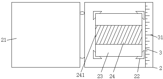
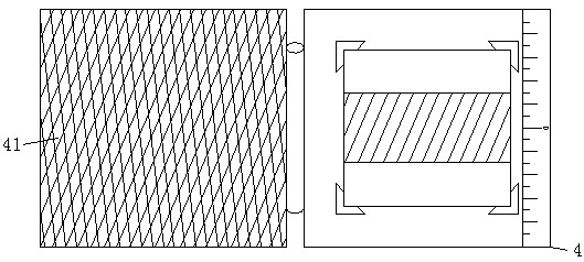
[0015] figure 2 It is a structural schematic diagram of the transparent mask box in the mask box that can measure the size of the mask protective film in the present invention; as figure 2 As shown, the present invention is a reticle box capable of measuring the size of the reticle protective film:

[0016] On the inner wall of the mask box 2 near the placement position of the mask plate, a scale 3 parallel to the extension line of the narrow side 421 of the mask plate protective film 42 on the mask plate 4 placed therein is provided. Wherein, the scale value of the scale 3 is on the order of millimeters, and the center line 31 of the scale 3 is on the same straight line as the center line of the narrow side 241 of the mask plate protective film 24, and the center of the scale is set as zero point, extending to both ends evenly set with the sa...


PUM


Abstract

The invention relates to the manufacturing field of a semiconductor, in particular to a mask plate box capable of measuring size of a mask plate protection film. Through the mask plate box capable of measuring the size of the mask plate protection film, a scale is arranged in the mask plate box; under the condition of not contacting the mask plate box, the size of the mask plate protection film can be simply and quickly measured; the risk of falsely using mask plates can be reduced; the step of judging through other equipment and tools can be omitted; and the process cost is saved.

Description

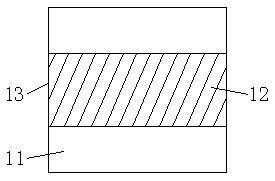
technical field [0001] The invention relates to the field of semiconductor integrated circuits and its manufacture, in particular to a mask box capable of measuring the size of a mask mask protective film. Background technique [0002] Since different types of lithography machines are used for different processes in the semiconductor chip manufacturing industry, mask plate protective films of different sizes are required for use in corresponding different types of lithography machines; figure 1 It is a schematic structural diagram of the mask plate in the background technology of the present invention; figure 1 As shown, the narrow side 13 of the mask plate protection film 12 disposed on the quartz plate 11 will vary in size with different types of photolithography machines. If the mask mask protective film of the wrong size is used, it will cause damage to the mask mask or the equipment. Therefore, the mask manufacturer will check the type of protective film used when the ...

Claims


Application Information

Patent Timeline
Patent Type & Authority Applications(China)
IPC IPC(8): H01L21/673
Inventor 戴韫青王剑毛智彪
Owner SHANGHAI HUALI MICROELECTRONICS CORP
Learn More