Check patentability & draft patents in minutes with Patsnap Eureka AI!
Manufacturing method of package with embedded chip
What is Al technical title?
Al technical title is built by PatSnap Al team. It summarizes the technical point description of the patent document.
A technology of embedded chips and manufacturing methods, which is applied in semiconductor/solid-state device manufacturing, electrical components, semiconductor devices, etc., and can solve problems such as cost increase, process time increase, and process difficulty
Active Publication Date: 2015-10-14
SILICONWARE PRECISION IND CO LTD
View PDF12 Cites 0 Cited by
Summary
Abstract
Description
Claims
Application Information
AI Technical Summary
This helps you quickly interpret patents by identifying the three key elements:
Problems solved by technology
Method used
Benefits of technology
Problems solved by technology
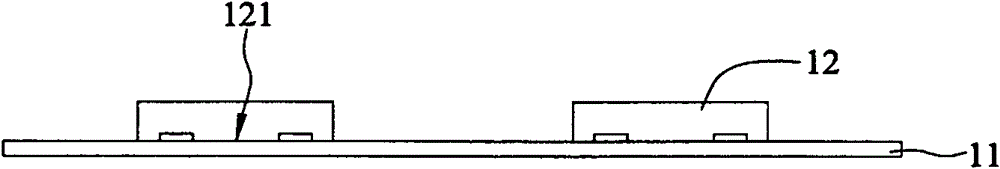
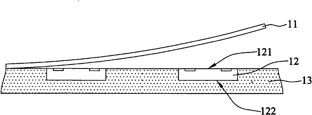
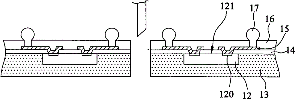
However, the process of penetrating the encapsulant 13 is difficult, and the conductive material 100 needs to be filled when forming the conductive via 10, so that the process time is increased and the cost is increased.
Method used
Image
Click on the blue label to locate the original text in one second.
Reading with bidirectional positioning of images and text.
Examples
Embodiment Construction
[0068] Embodiments of the present invention are described below through specific examples, and those skilled in the art can easily understand other advantages and effects of the present invention from the content disclosed in this specification.
[0069] It should be noted that the structures, proportions, sizes, etc. shown in the drawings of this specification are only used to match the content disclosed in the specification for the understanding and reading of those skilled in the art, and are not used to limit the conditions for the implementation of the present invention , so it has no technical substantive meaning, and any modification of structure, change of proportional relationship or adjustment of size shall still fall within the scope of the disclosure of the present invention without affecting the functions and objectives of the present invention. within the range covered by the technical content. At the same time, terms such as "above" and "one" quoted in this spec...
PUM
Abstract
The invention relates to a package of an embedded chip and a manufacturing method thereof. The package comprises: a dielectric layer, which has a first surface and a second surface that is opposite to the first surface; conductive projections, which are arranged in the dielectric layer and are exposed outside the dielectric layer; a chip, which is embedded in the dielectric layer; a line layer, which is arranged on the first surface of the dielectric layer; conductive blind holes, which are arranged in the dielectric layer and are electrically connected with the line layer, the chip and the conductive projection; and a first welding-resistant layer, which is arranged on the first surface of the dielectric layer and the line layer. Therefore, other electronic apparatuses can be externally connected by the conductive projections, so that a stacked structure is formed; and the technology is effectively simplified. In addition, the invention also provides a manufacturing method of a chip scale package.
Description
technical field [0001] The invention relates to a package and its manufacturing method, in particular to an embedded chip package and its manufacturing method. Background technique [0002] With the evolution of semiconductor technology, semiconductor products have developed different packaging product types, and in order to pursue the lightness, thinness and shortness of semiconductor packages, a chip scale package (CSP) has been developed, which is characterized in that Chip-scale packages are only equal to or slightly larger than the chip size. [0003] U.S. Patent Nos. 5,892,179, 6,103,552, 6,287,893, 6,350,668 and 6,433,427 disclose a traditional CSP structure, which directly forms build-up layers on the chip without using chip carriers such as substrates or lead frames, and uses redistribution layer, RDL) technology to reconfigure the electrode pads on the chip to the desired position. [0004] However, the disadvantage of the above-mentioned CSP structure is that th...
Claims
Application Information
Patent Timeline
Application Date:The date an application was filed.
Publication Date:The date a patent or application was officially published.
First Publication Date:The earliest publication date of a patent with the same application number.
Issue Date:Publication date of the patent grant document.
PCT Entry Date:The Entry date of PCT National Phase.
Estimated Expiry Date:The statutory expiry date of a patent right according to the Patent Law, and it is the longest term of protection that the patent right can achieve without the termination of the patent right due to other reasons(Term extension factor has been taken into account ).
Invalid Date:Actual expiry date is based on effective date or publication date of legal transaction data of invalid patent.
