tft-lcd, driving device and manufacturing method thereof

A technology of driving devices and thin film transistors, which is applied in the field of flat panel displays, can solve the problems of large size of driving devices, achieve the effect of ensuring driving ability and reducing size

Inactive Publication Date: 2014-10-22
BEIJING BOE OPTOELECTRONCIS TECH CO LTD
View PDF6 Cites 0 Cited by
  • Summary
  • Abstract
  • Description
  • Claims
  • Application Information

AI Technical Summary

Problems solved by technology

[0004] The invention provides a TFT-LCD, a driving device and a manufacturing method thereof, which are used to solve the problem of large size of the driving device in the prior art, and can reduce the area occupied by the driving device on the array substrate while ensuring the driving capability of the driving device

Method used


Image

  • tft-lcd, driving device and manufacturing method thereof
  • tft-lcd, driving device and manufacturing method thereof
  • tft-lcd, driving device and manufacturing method thereof

Examples


Embodiment Construction

[0041] In order to make the purpose, technical solutions and advantages of the embodiments of the present invention clearer, the technical solutions in the embodiments of the present invention will be clearly and completely described below in conjunction with the drawings in the embodiments of the present invention. Obviously, the described embodiments It is a part of embodiments of the present invention, but not all embodiments. Based on the embodiments of the present invention, all other embodiments obtained by persons of ordinary skill in the art without creative efforts fall within the protection scope of the present invention.

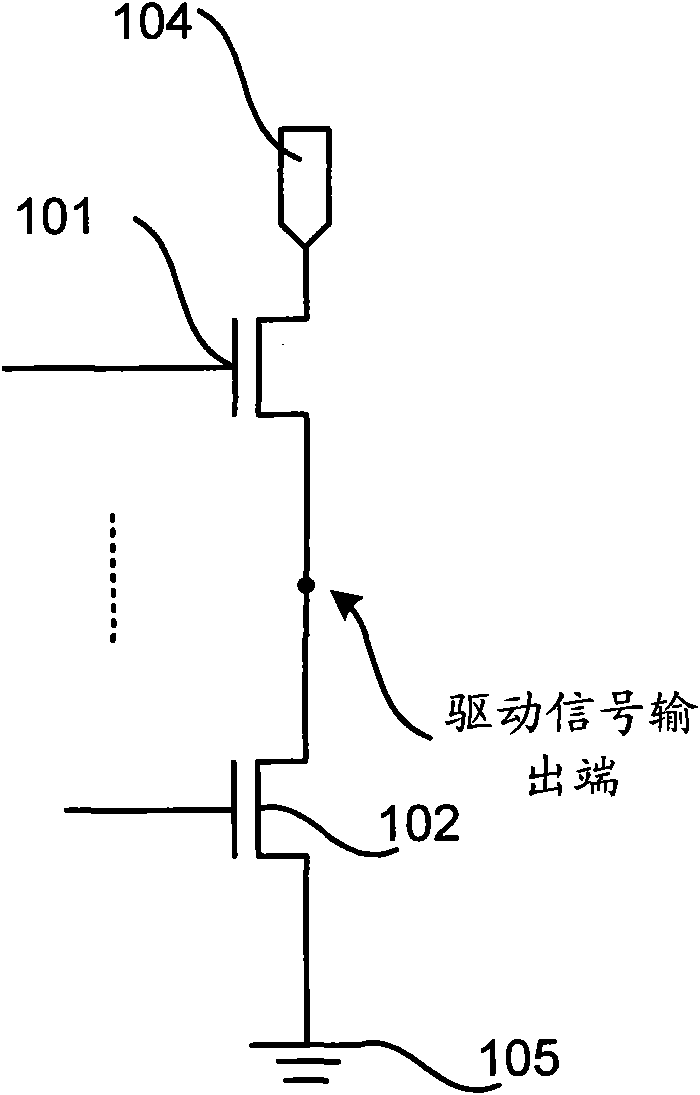
[0042] Such as figure 1 Shown is a schematic structural diagram of the first embodiment of the TFT-LCD driving device of the present invention, including at least one first thin film transistor 101 and at least one second thin film transistor 102 formed on the array substrate, the load of the first thin film transistor 101 is greater than that of ...


PUM


Abstract

An embodiment of the disclosed technology provides a driving device for a thin film transistor liquid crystal display (TFT-LCD) and a method for manufacturing the same. The driving device comprises at least one first TFT and at least one second TFT formed a base substrate, wherein load of the first TFT is larger than load of the second TFT, the first TFT is of a top-gate configuration, and the second TFT is of a bottom-gate configuration.

Description

technical field [0001] The present invention relates to the technical field of flat panel displays, in particular to a Thin Film Transistor Liquid Crystal Display (TFT-LCD for short), a driving device and a manufacturing method thereof. Background technique [0002] Most of the driving devices in the TFT-LCD are implemented by a silicon integrated circuit (Silicon Integrated Circuit, IC for short). In recent years, with the continuous improvement of the thin film transistor technology, the technology of integrating the thin film transistor on the array substrate of the TFT-LCD to form the driving device has gradually appeared. For example, a gate line driving device, a data line driving device and the like made of amorphous silicon thin film transistors can be formed on the array substrate. [0003] When amorphous silicon thin film transistors are used to form driving devices, some thin film transistors need to have strong driving capabilities. In order to achieve a strong...

Claims


Application Information

Patent Timeline
Patent Type & Authority Patents(China)
IPC IPC(8): G02F1/1368G02F1/133H01L27/02H01L21/77
CPCH01L29/4908H01L29/458H01L27/1251G11C19/28
Inventor 曹昆胡明
Owner BEIJING BOE OPTOELECTRONCIS TECH CO LTD
Why Eureka
Try Eureka