An Asymmetric Dual-Gate Junctionless Field-Effect Transistor

A junction field effect, asymmetric technology, used in semiconductor devices, electrical components, circuits, etc., to achieve the effect of large turn-on current, large gate control capability, and good turn-off current

Active Publication Date: 2018-12-25
HANGZHOU DIANZI UNIV
View PDF2 Cites 0 Cited by
  • Summary
  • Abstract
  • Description
  • Claims
  • Application Information

AI Technical Summary

Problems solved by technology

[0004] However, when the size of the device is reduced to a greater extent (approaching less than 20nm), the characteristics of the junction-free device will also show many shortcomings.

Method used


Image

  • An Asymmetric Dual-Gate Junctionless Field-Effect Transistor
  • An Asymmetric Dual-Gate Junctionless Field-Effect Transistor
  • An Asymmetric Dual-Gate Junctionless Field-Effect Transistor

Examples


Embodiment Construction

[0015] In order to make the purpose, technical solution and advantages of the present invention clearer, the present invention will be described in detail below in conjunction with the accompanying drawings.

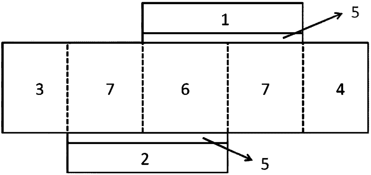
[0016] Such as figure 1 As shown, a new type of asymmetric double gate junctionless field effect transistor, including top gate 1, bottom gate 2, source region 3, drain region 4, gate dielectric layer 5, channel overlapping region 6, channel non-overlapping Region 7; wherein, the top gate 1 and the bottom gate 2 are located above and below the channel, and have an asymmetric structure; there is an overlapping area between the top gate 1 and the bottom gate 2; the channel overlap area 6; the channel overlap area 6 is located between the channel non-overlapping region 7, the source region 3 and the drain region 4 are located on both sides of the channel non-overlapping region 7, between the top gate 1 and the channel, and between the bottom gate 2 and the channel respectiv...


PUM


Abstract

The invention discloses a novel asymmetric double-gate junctionless field effect transistor comprising a top gate, a bottom gate, a source region, a drain region, gate dielectric layers, a channel overlap region, and channel non-overlap regions. The top gate and the bottom gate are respectively disposed in an upper position and in a lower position of a channel, and are of an asymmetric structure. There is an overlap region between the top gate and the bottom gate, namely, the channel overlap region. The channel overlap region is between the channel non-overlap regions. The source region and the drain region are respectively disposed at the two sides of the channel non-overlap regions. The gate dielectric layers are respectively arranged between the top gate and the channel and between the bottom gate and the channel. Because of the asymmetric gate structure, smaller channel length is achieved when the device is opened, and larger channel length is achieved when the device is closed. The structure can ensure that the novel device has higher closing current and greater gate control capability at the closing moment and has higher opening current at the opening moment.

Description

technical field [0001] The invention relates to a device for semiconductor integrated circuits, mainly a novel asymmetric double-gate junction-free field-effect transistor. Background technique [0002] As the size of CMOS devices shrinks, junctionless devices are a good device structure to meet the challenges of size reduction. For CMOS devices, a good transfer characteristic curve is very important, which mainly depends on the subthreshold slope (SS) of the device, the leakage-induced barrier lowering (DIBL) characteristics, the size of the threshold voltage, the leakage current (I OFF ) size, drive current (I ON ) and other factors. These characteristics belong to the basic electrical characteristics of the device. In addition, junctionless devices also have other characteristics that need to be studied, such as variability, reliability, AC characteristics, and so on. Junctionless devices encounter many variability problems when shrinking in size, such as threshold vo...

Claims


Application Information

Patent Timeline
Patent Type & Authority Patents(China)
IPC IPC(8): H01L29/78H01L29/423
CPCH01L29/4232H01L29/42356H01L29/7831
Inventor 王颖孙玲玲唐琰曹菲
Owner HANGZHOU DIANZI UNIV
Why Eureka
Try Eureka