Method for manufacturing metal oxide semiconductor field effect transistor and device thereof

A technology of oxide semiconductors and field effect transistors, which is applied in the field of semiconductor manufacturing methods and devices, can solve problems such as huge investment, and achieve the effect of reducing the channel length

Active Publication Date: 2013-12-04
SHANGHAI HUAHONG GRACE SEMICON MFG CORP
View PDF0 Cites 0 Cited by
  • Summary
  • Abstract
  • Description
  • Claims
  • Application Information

AI Technical Summary

Problems solved by technology

Upgrading lithography equipment requires huge investment

Method used


Image

  • Method for manufacturing metal oxide semiconductor field effect transistor and device thereof
  • Method for manufacturing metal oxide semiconductor field effect transistor and device thereof
  • Method for manufacturing metal oxide semiconductor field effect transistor and device thereof

Examples


Embodiment Construction

[0028] In order to understand the technical content of the present invention more clearly, specific embodiments are given and described as follows in conjunction with the accompanying drawings.

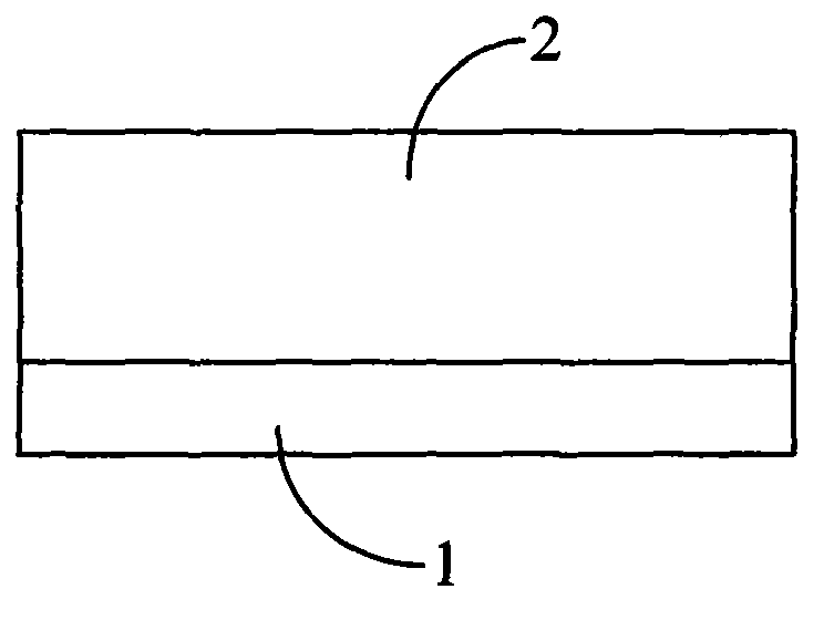
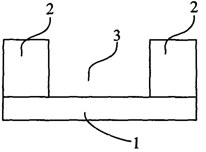
[0029] see Figure 1A , provide a semiconductor substrate 1, optionally, as required, the semiconductor substrate 1 is a P-type substrate, or an N-type substrate, and a P well (NMOS) or an N well ( PMOS), and then an insulating layer 2 is formed on the surface of the semiconductor substrate 1 by deposition, such as Figure 1B shown. The insulating layer 2 is silicon oxide, nitride or a combination of oxide and nitride, such as silicon dioxide (SiO 2 ), silicon nitride (SiN), or other dielectrics.

[0030] Then, a groove 3 is etched on the insulating layer 2 by etching to expose the semiconductor substrate 1, such as Figure 1C shown.

[0031] Next, on the groove 3, ion implantation is used to implant the groove 3 at an oblique angle, thereby forming a lightly doped drain region (...


PUM


Abstract

The invention discloses a method for manufacturing a metal oxide semiconductor field effect transistor and a device thereof. The manufacturing method comprises the following steps: providing a semiconductor substrate; forming an insulating layer on the surface of the semiconductor substrate; forming a groove on the insulating layer; forming light dope drain regions in the semiconductor substrate below the lateral wall of the groove respectively; forming grid flank walls on the lateral wall of the groove respectively; forming grid dielectric layers on the groove surfaces between the grid flank walls; forming grids in an accommodating space encircled by the grid flank walls and the grid dielectric layers; removing the insulating layer; and forming a source region and a drain region respectively in the semiconductor substrates on two sides of the grid flank walls. The manufacturing method breaks through the limitation of the minimum grid length which can be achieved by a photoetching device, and reduces the length of a channel formed between the source region and the drain region; and the device formed according to the method is helpful for enhancing the firing current and reducing the electric leakage caused by short-channel effect.

Description

technical field [0001] The invention relates to a semiconductor manufacturing method and its device, in particular to a metal oxide semiconductor field effect transistor manufacturing method and its device. Background technique [0002] With the advancement of semiconductor technology, semiconductor devices with lower cost, lower power consumption and faster speed have become one of the goals generally pursued by the semiconductor and electronics industries. In order to achieve the above goals, increase the integration level, reduce the unit area, and manufacture more transistors in the same chip area, the size of semiconductor devices needs to continue to shrink with the development of technology, and the gate length becomes shorter. In order to obtain a shorter gate length, the usual method is to upgrade the lithography equipment. At present, lithography machines have become the most expensive equipment in semiconductor manufacturing, and the price of a 193nm lithography ...

Claims


Application Information

Patent Timeline
Patent Type & Authority Patents(China)
IPC IPC(8): H01L21/336H01L21/265H01L29/78H01L29/08H01L29/10
Inventor 孔蔚然
Owner SHANGHAI HUAHONG GRACE SEMICON MFG CORP
Why Eureka
Try Eureka