

MOSFET and its manufacture
An oxide semiconductor and field effect transistor technology, which is applied in the field of metal oxide semiconductor field effect transistors and their manufacturing, can solve the problems such as the deterioration of the surface properties of the channel region, the difficulty of the planarization process, and the impact on the performance of the components. The effect of easily controlled conditions
- Summary
- Abstract
- Description
- Claims
- Application Information
AI Technical Summary
Problems solved by technology
Method used
Image

Examples
Embodiment Construction
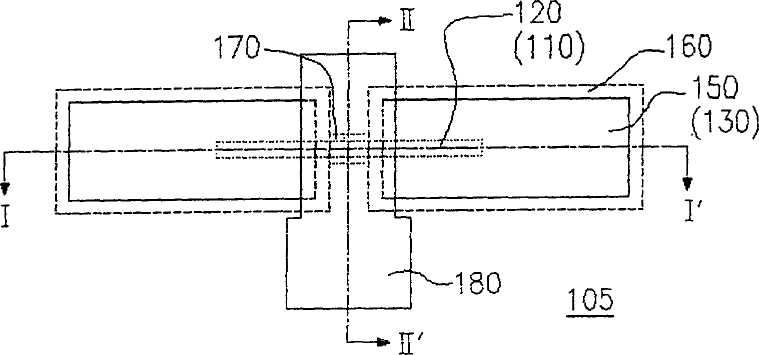
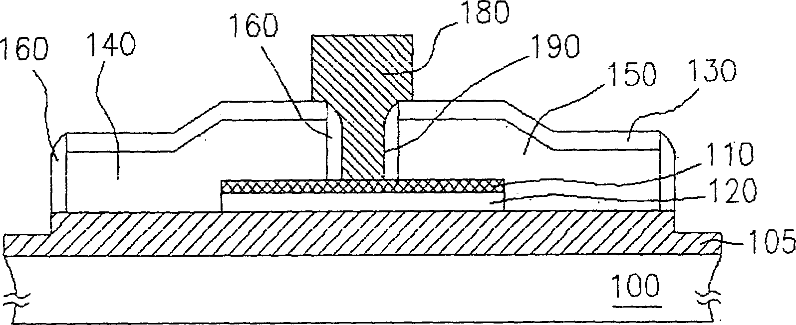
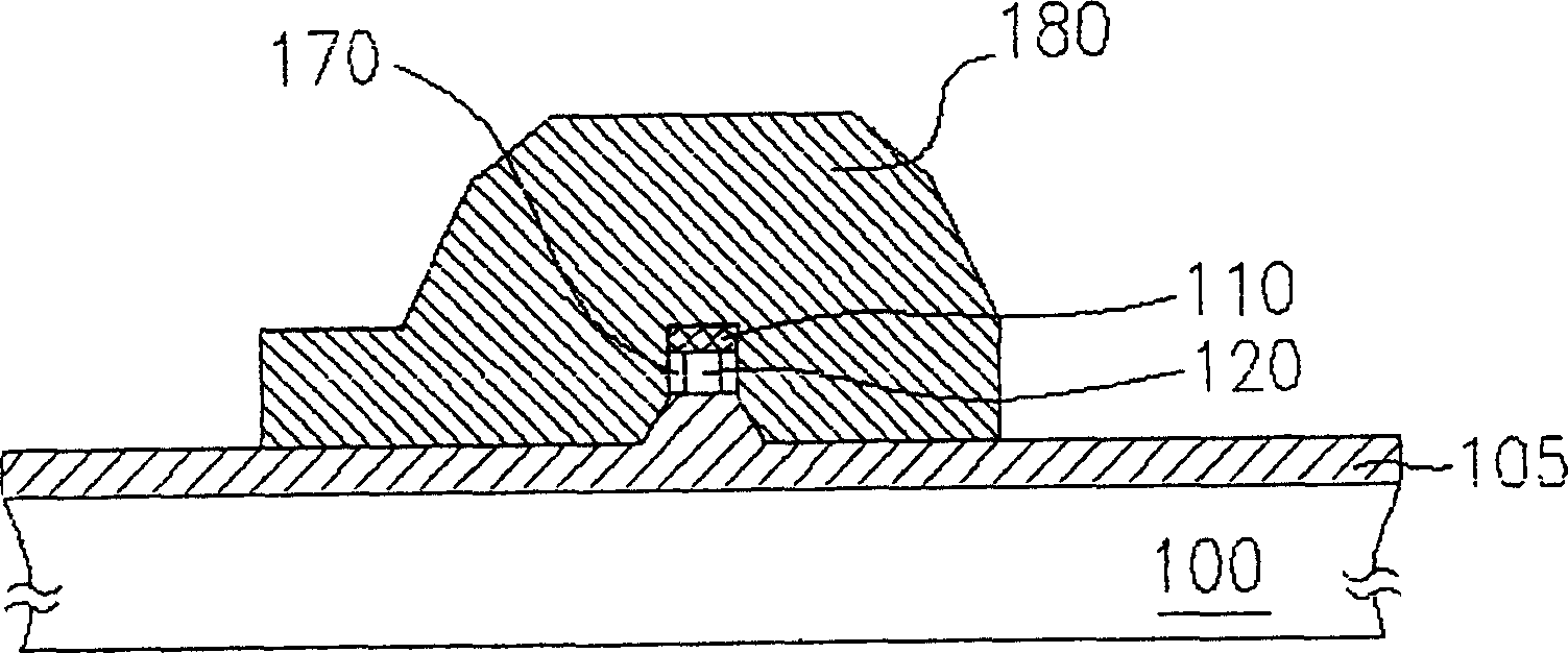
[0074] Please refer to Figure 2 to Figure 9 , which shows a cross-sectional view of the manufacturing process of a metal-oxide-semiconductor field-effect transistor in a preferred embodiment of the present invention; and please refer to Figure 2A , 5A , 6A, 8A, which are respectively figure 2 , 5 , the top view of 6, 8, and figure 2 , 5 , 6, and 8 are respectively Figure 2A , 5A , 6A, 8A section view of cutting line III-III'. in addition Figure 8B for Figure 8A Sectional view of cutting line IV-IV'.
[0075] Please refer to figure 2 , 2 A, where figure 2 for Figure 2A Sectional view of cutting line III-III'. Such as figure 2 , 2 As shown in A, first provide a semiconductor substrate 200, which is, for example, a bulky silicon substrate, and then form a ring-shaped shallow trench isolation 210 (Shallow Trench Isolation, STI) on it, the material of which is, for example, high Silicon oxide formed by density plasma chemical vapor deposition (HDP-CVD). ...
PUM
 Abstract
Description
Claims
Application Information