No-junction field effect transistor and manufacturing method therefor

A production method and junction field effect technology, applied in semiconductor/solid-state device manufacturing, electrical components, circuits, etc., can solve problems such as large contact resistance, small size, and exacerbated MOSFET short channel effect, so as to improve performance and reduce The effect of interface scattering

Inactive Publication Date: 2016-03-30
SEMICON MFG INT (SHANGHAI) CORP
View PDF8 Cites 0 Cited by
  • Summary
  • Abstract
  • Description
  • Claims
  • Application Information

AI Technical Summary

Problems solved by technology

However, as the feature size decreases, the difficulty of the doping process increases, and as the difficulty of the doping process increases, it becomes more difficult to reduce the resistance between the source and drain regions through doping, while reducing the size of the gate It means that the size of the channel region is correspondingly smaller, which may exacerbate the short channel effect of MOSFET
[0005] In addition, since the source and drain regions of the MOSFET in the prior art are all doped semiconductor materials, when the conductive plugs connected to the source and drain regions are subsequently formed, there is a gap between the conductive plugs (usually metal materials) and the source and drain regions. There is a large contact resistance
[0006] Problems such as transistor leakage, large resistance between source and drain regions, and large contact resistance between conductive plugs and source and drain regions affect the performance of transistors

Method used


Image

  • No-junction field effect transistor and manufacturing method therefor
  • No-junction field effect transistor and manufacturing method therefor
  • No-junction field effect transistor and manufacturing method therefor

Examples


Embodiment Construction

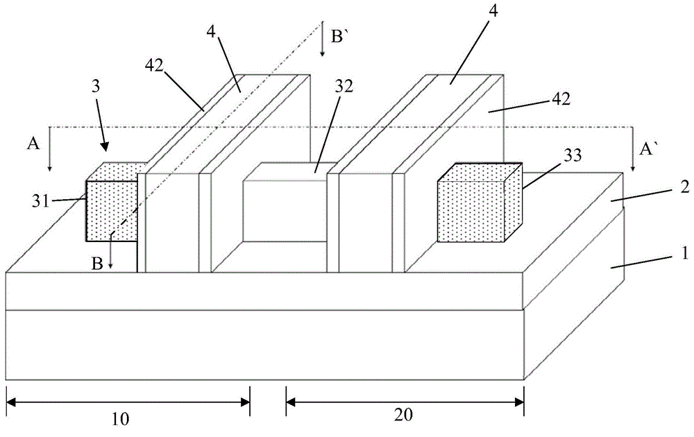
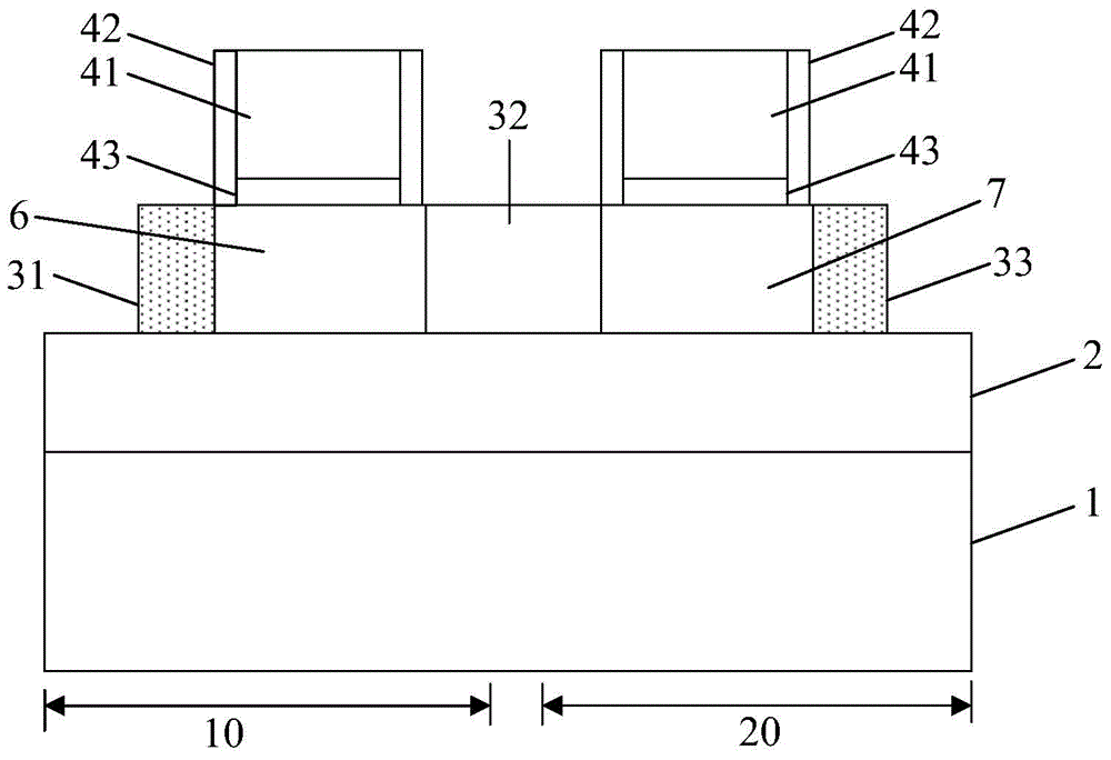
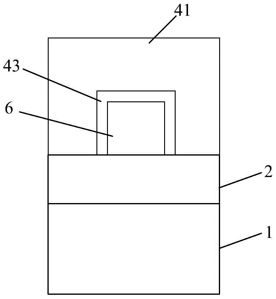
[0067] Since the feature size of existing field effect transistors (such as MOSFETs) decreases gradually, the difficulty of the doping process for making MOSFETs also gradually increases; at the same time, since the source and drain regions of existing MOSFETs are generally semiconductor materials, the source and drain The problem of large resistance between regions has been difficult to improve; and there is a large contact resistance between the semiconductor material and the conductive plug in the interconnect structure, generally requiring additional process steps to form a low contact resistance on the source and drain regions. silicide contact layer.

[0068] In addition, when the MOSFET is working, the interface scattering (surface scattering) phenomenon of carriers in the channel region is relatively serious, which will affect the working performance of the junctionless field effect transistor to a certain extent, such as increased noise.

[0069] Therefore, the presen...


PUM

PropertyMeasurementUnit
thicknessaaaaaaaaaa
thicknessaaaaaaaaaa
thicknessaaaaaaaaaa

Abstract

The invention discloses a no-junction field effect transistor and a manufacturing method therefor, and the method comprises the steps: providing a substrate; carrying out the doping so as to form a first doping region and a second doping region and to enable the doping types of the first and second doping regions to be different; forming a first grid structure and a second grid structure; removing a part of substrate, so as to form a first opening and a second opening; forming metal layers in the first and second openings; and carrying out the annealing of the metal layers and the substrate, so as to form source-drain regions. The invention also provides a no-junction field effect transistor, and the field effect transistor comprises the substrate; the first doping region and the second doping region; the first grid structure and the second grid structure; and the first and second openings, wherein the interiors of the first and second openings are provided with material layers containing metal, and the material layers serve as the source-drain regions. The beneficial effects of the invention lie in that the contact resistance between the source-drain regions and a conductive plug is smaller; the starting current is increased; the performance of the no-junction field effect transistor is improved; the technological difficulty is simplified; and the degree of interface scattering which may happen in the doping regions is reduced to some degree.

Description

technical field [0001] The invention relates to the field of semiconductor manufacturing, in particular to a junctionless field effect transistor and a manufacturing method thereof. Background technique [0002] Metal-Oxide Semiconductor Field Effect Transistor (MetalOxideSemiconductorFieldEffectTransistor, MOSFET) in addition to the source and drain regions, the gate, there are also channel junctions such as PN junctions, heterojunctions, etc. in the channel region between the source and drain regions (junction). [0003] As the feature size of MOSFETs gradually decreases, more and more problems begin to emerge. For example, as the size of the MOSFET decreases, the degree of leakage of the MOSFET during operation increases. [0004] In addition, in order to further improve the performance of the MOSFET, it is also one of the more critical issues to minimize the resistance between the source and drain regions. In general, reducing the size of the gate or adjusting the dop...

Claims


Application Information

Patent Timeline
Patent Type & Authority Applications(China)
IPC IPC(8): H01L21/336H01L29/78H01L29/06H01L29/423
Inventor 肖德元
Owner SEMICON MFG INT (SHANGHAI) CORP
Why Eureka
Try Eureka