TFT (Thin Film Transistor) array substrate, manufacturing method and liquid crystal display device
An array substrate and substrate technology, applied in the field of manufacturing methods, liquid crystal display devices, and TFT array substrates, can solve the problems of affecting picture quality, not being able to completely guarantee shading, and increasing manufacturing costs, etc.
- Summary
- Abstract
- Description
- Claims
- Application Information
AI Technical Summary
Problems solved by technology
Method used
Image


Examples
Embodiment Construction
[0030] The following will clearly and completely describe the technical solutions in the embodiments of the present invention with reference to the accompanying drawings in the embodiments of the present invention. Obviously, the described embodiments are only some, not all, embodiments of the present invention. Based on the embodiments of the present invention, all other embodiments obtained by persons of ordinary skill in the art without making creative efforts belong to the protection scope of the present invention.
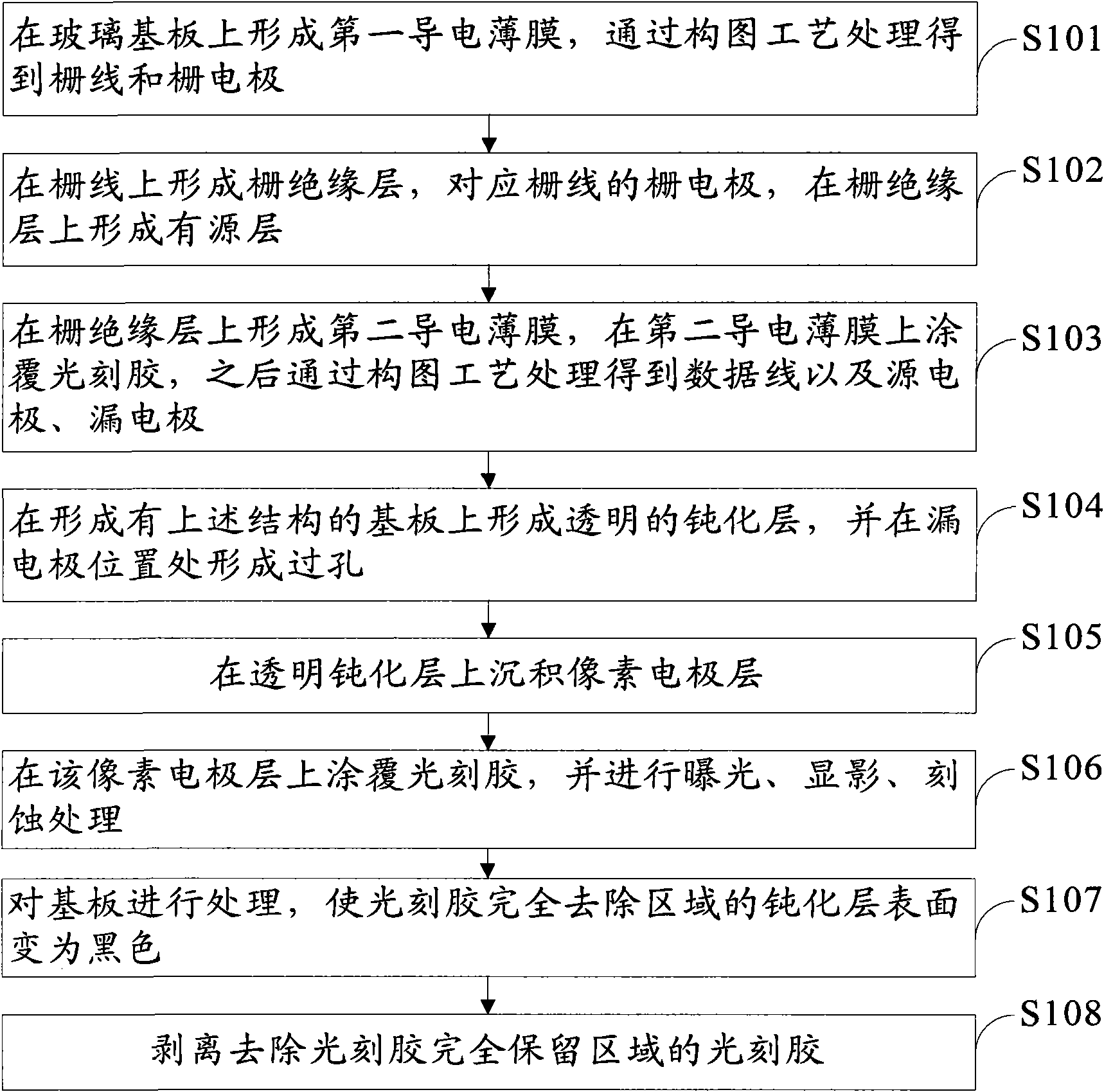
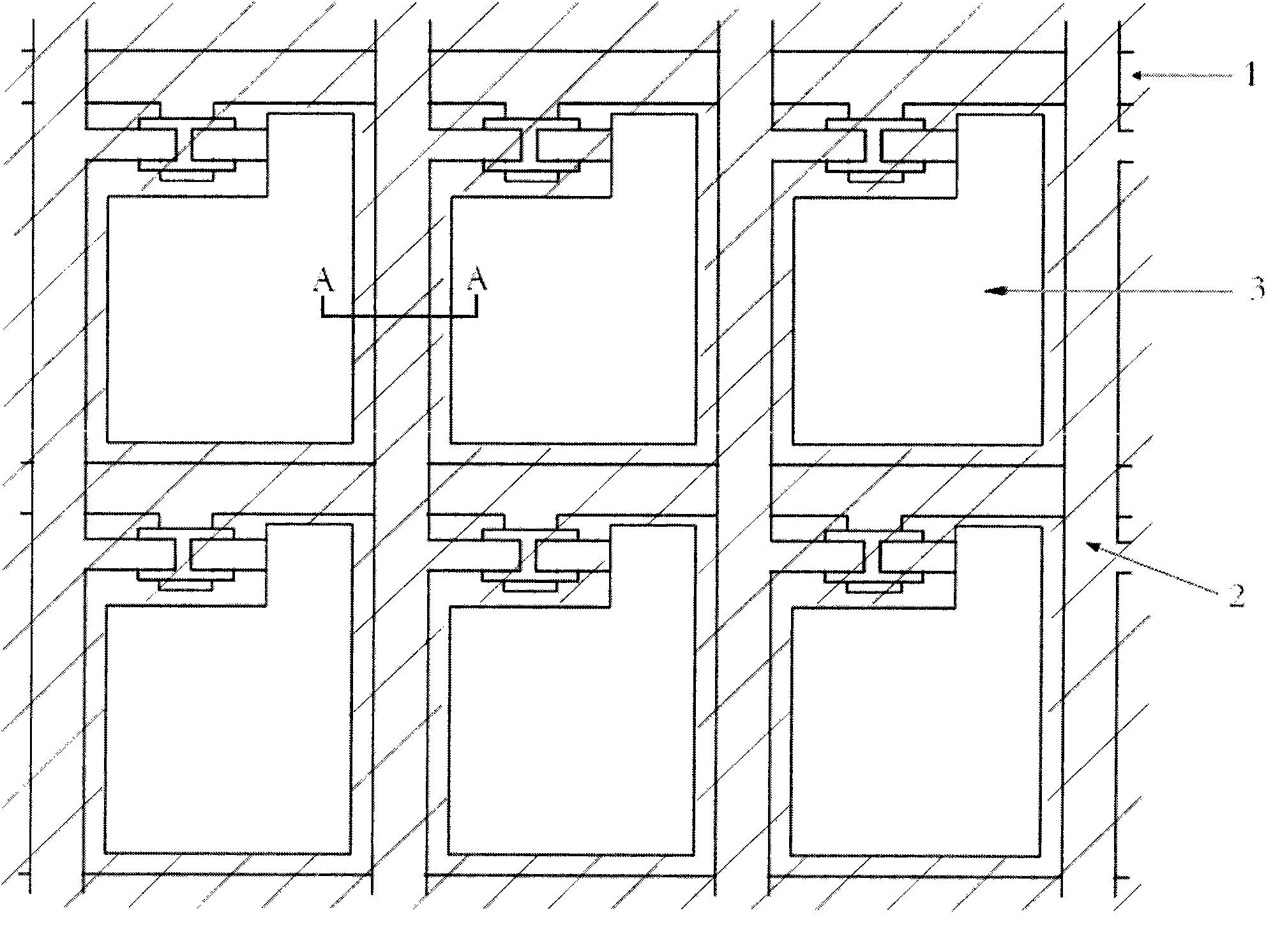
[0031] The TFT array substrate manufacturing method provided by the embodiment of the present invention, such as figure 1 As shown, the steps include:
[0032] S101 , forming a first conductive film on a glass substrate, and obtaining gate lines and gate electrodes through a patterning process.
[0033] Specifically, a metal thin film with a thickness of 1000 to 7000 Å can be prepared on a glass substrate by using a magnetron sputtering method. The metal mat...
PUM
 Abstract
Description
Claims
Application Information
 - R&D Engineer
- R&D Manager
- IP Professional
- Industry Leading Data Capabilities
- Powerful AI technology
- Patent DNA Extraction
Browse by: Latest US Patents, China's latest patents, Technical Efficacy Thesaurus, Application Domain, Technology Topic.
© 2024 PatSnap. All rights reserved.Legal|Privacy policy|Modern Slavery Act Transparency Statement|Sitemap