Supercharge Your Innovation With Domain-Expert AI Agents!

Perfect printing device for printed circuit boards (PCBs)

A double-sided printing and PCB board technology, which is applied in printing, printing machines, rotary printing machines, etc., can solve the problems of sticking to the screen printing table, insecure quality, and low efficiency, so as to improve processing efficiency and shorten the baking time. Effect

Inactive Publication Date: 2012-06-13
常州市双进电子有限公司
View PDF0 Cites 1 Cited by
  • Summary
  • Abstract
  • Description
  • Claims
  • Application Information

AI Technical Summary

Problems solved by technology

In order to prevent the problems of baked to death and unclean development, the conventional method: first print one side to dry and then print the second side; but the first baking time should not exceed 25 minutes, this method can also be produced, but has the following disadvantages: When printing the second side, it may stick to the screen printing table and lose oil, low efficiency and no guarantee of quality

Method used


Image

  • Perfect printing device for printed circuit boards (PCBs)
  • Perfect printing device for printed circuit boards (PCBs)

Examples


Embodiment Construction

[0010] The present invention will now be described in further detail in conjunction with the accompanying drawings and preferred embodiments. These drawings are all simplified schematic diagrams, which only illustrate the basic structure of the present invention in a schematic manner, so they only show the configurations related to the present invention.

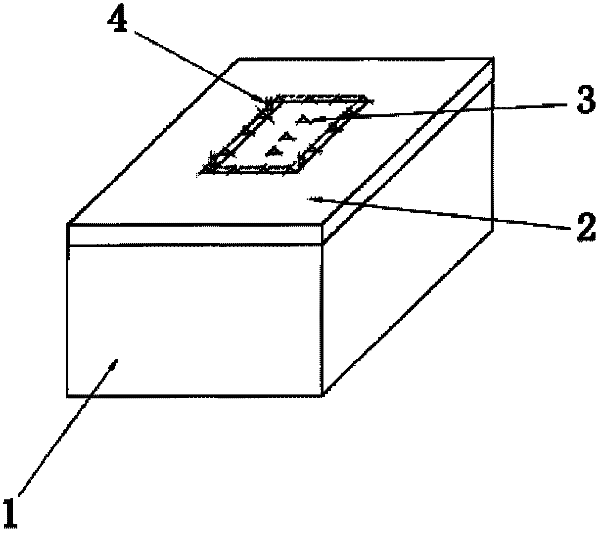
[0011] like figure 1 A PCB board double-sided printing device is shown, which is mainly used for solder masking on both sides of the PCB board. During double-sided printing, it prevents the lower board from sticking to the screen printing table and oil loss caused by the adhesion of the lower board to the screen printing table. . Wherein said PCB double-sided printing device mainly includes a silk screen printing table 1, which is provided with a silk screen printing table 2 on the silk screen printing table 2, and positioning nails 4 are distributed on the silk screen printing table 2, and the positioning nails 4 here are ...


PUM


Abstract

The invention relates to a perfect printing device for printed circuit boards (PCBs), which comprises a silk screen table and a table board arranged on the silk screen table. Location nails are arranged on the table board. Due to the fact that the location nails are positioned on the silk screen table, and copper nails are distributed in an area formed by the location nails, a nail bed is formed on the silk screen table, the other sides of the PCBs are prevented from being in contact with the silk screen table during the process that second sides of the PCBs are printed, one-side printing and two-side solder resistance can be achieved in one time, time for baking board is greatly shortened, and processing efficiency is improved.

Description

technical field [0001] The invention relates to a PCB double-sided printing device. Background technique [0002] With the development of multi-function and miniaturization of electronic equipment, more functions need to be carried on the circuit board. Therefore, the direction of double-sided wiring is moving forward when the single-sided wiring cannot carry it. At present, the interconnection of double-sided patterns often adopts the through-plating method, which uses through-hole plating and etching of copper foil to remove partially useless copper foil on the surface of the substrate, thereby forming a non-conductor substrate surface. [0003] PCB boards are printed on one side when printing solder resist and text. Since the photosensitive solder resist ink is baked in the oven for a long time, it will cause problems such as baked to death and dirty development. Therefore, the use of a double-sided printing device can improve production efficiency and reduce the number ...

Claims


Application Information

Patent Timeline
Patent Type & Authority Applications(China)
IPC IPC(8): B41F15/08H05K3/28
Inventor 张南松
Owner 常州市双进电子有限公司
Features
  • R&D
  • Intellectual Property
  • Life Sciences
  • Materials
  • Tech Scout
  • Unparalleled Data Quality
  • Higher Quality Content
  • 60% Fewer Hallucinations
Learn More