

Method for determining service life of hot carrier injection device
A hot carrier, device life technology, applied in the direction of single semiconductor device testing, etc.
- Summary
- Abstract
- Description
- Claims
- Application Information
AI Technical Summary
Problems solved by technology
Method used
Image

Examples
Embodiment Construction
[0025] In order to make the above objects, features and advantages of the present invention more comprehensible, specific implementations of the present invention will be described in detail below in conjunction with the accompanying drawings.
[0026] In the following description, numerous specific details are set forth in order to provide a thorough understanding of the present invention. However, the present invention can be implemented in many other ways different from those described here, and those skilled in the art can make similar extensions without violating the connotation of the present invention, so the present invention is not limited by the specific implementations disclosed below.
[0027] see figure 1 , a method for determining the lifetime of a hot carrier injection device provided by the present invention is as follows:
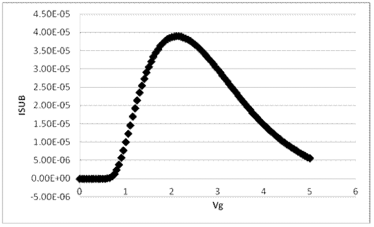
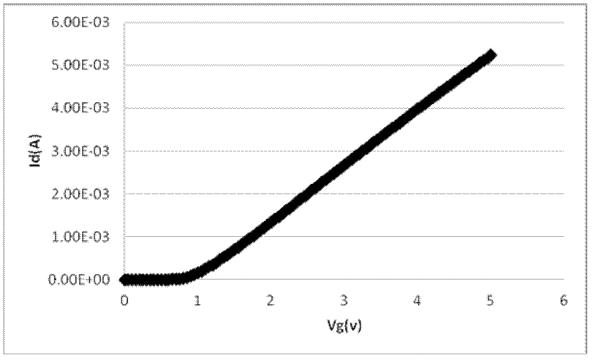
[0028] Step 1: Select a MOS device, conduct a hot carrier injection experiment on the MOS device, and measure the substrate current and g...
PUM
 Abstract
Description
Claims
Application Information