Photonic crystal wavelength division multiplexer

A technology of wavelength division multiplexer and photonic crystal, which is applied in light guides, optics, instruments, etc., can solve the problems of low transmittance and low actual efficiency of wavelength division multiplexing, and achieve good frequency selection characteristics and high transmittance. high effect

Inactive Publication Date: 2013-05-01
INST OF SEMICONDUCTORS - CHINESE ACAD OF SCI
View PDF6 Cites 2 Cited by
  • Summary
  • Abstract
  • Description
  • Claims
  • Application Information

AI Technical Summary

Problems solved by technology

Because the waveguide structure involves a 90-degree curved waveguide, generally the transmittance of the curved waveguide itself is not high, resulting in the actual efficiency of the wavelength division multiplexing is not high

Method used


Image

  • Photonic crystal wavelength division multiplexer
  • Photonic crystal wavelength division multiplexer
  • Photonic crystal wavelength division multiplexer

Examples


Embodiment Construction

[0022] In order to make the object, technical solution and advantages of the present invention clearer, the present invention will be described in further detail below in conjunction with specific embodiments and with reference to the accompanying drawings.

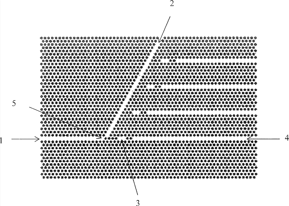
[0023] The photonic crystal wavelength division multiplexer provided by the present invention uses photonic crystals with different lattice parameters to be continuously spliced ​​together to form a photonic crystal heterojunction, and removes a row of air holes in the photonic crystal heterojunction to form a photonic crystal heterojunction waveguide ; The photonic crystal microcavity is set in the transmission waveguide to realize the resonant coupling between the microcavity waveguides. Theoretically research the coupling of photonic crystal microcavity and photonic crystal waveguide to realize the wavelength division multiplexing method, and structurally adopt the resonant coupling method of photonic crystal heterojunc...


PUM


Abstract

The invention discloses a photonic crystal wavelength division multiplexer. The photonic crystal wavelength division multiplexer adopts the structure of a two-dimensional photonic crystal with triangular crystal lattices, and comprises a photonic crystal input straight waveguide, a 60-degree oblique waveguide, photonic crystal microcavities and photonic crystal output straight waveguides, whereinan optical signal is input through the photonic crystal input straight waveguide and forms the 60-degree oblique waveguide in the direction of a regularly triangular 60-degree angle after transversely transmitting for about tens of periods; two or three holes are removed at the positions close to the transverse direction of the 60-degree oblique waveguide at the interval of three holes to form the photonic crystal microcavities; then other holes in the rows are removed to form the photonic crystal output straight waveguides after two or three holes are remained, so as to form a curved waveguide-microcavity-straight waveguide structure; and 10 to 20 rows of holes are formed between every two microcavity-straight waveguide structures at intervals. In the invention, the photonic crystal straight waveguides, the curved waveguides and the photonic crystal microcavities are coupled to achieve filtering and select signals with specific wavelengths to serve a wave division function.

Description

technical field [0001] The invention relates to the technical fields of photonic integration, optical communication, photonic crystal filter, etc., in particular to a photonic crystal wavelength division multiplexer which utilizes photonic crystal microcavity and waveguide coupling to realize optical signal separation, filtering and wave combining. Background technique [0002] With the rapid development of the information society, information technology requires the scale of integrated circuits to be larger and larger, and the volume of electronic components is required to be smaller and smaller. But as individual components get smaller and circuits get more complex, electrons are moving closer and closer to their limit speed. Therefore, it is becoming more and more important to develop a new generation of information technology. Due to the fast running speed of photons and the absence of mutual interference between photons, photon integration has become an important choic...

Claims


Application Information

Patent Timeline
Patent Type & Authority Patents(China)
IPC IPC(8): G02B6/122
Inventor 许兴胜
Owner INST OF SEMICONDUCTORS - CHINESE ACAD OF SCI
Why Eureka
Try Eureka